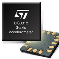
LIS3LV02DL STMicroelectronics, LIS3LV02DL Datasheet - Page 23

LIS3LV02DL
Manufacturer Part Number
LIS3LV02DL
Description
Board Mount Accelerometers MEMS INERTIAL SENSOR
Manufacturer
STMicroelectronics
Datasheet
1.LIS3LV02DL.pdf
(48 pages)
Specifications of LIS3LV02DL
Sensing Axis
X, Y, Z
Acceleration
2 g, 6 g
Digital Output - Number Of Bits
12 bit, 16 bit
Supply Voltage (max)
3.6 V
Supply Voltage (min)
2.16 V
Supply Current
0.65 mA
Maximum Operating Temperature
+ 85 C
Minimum Operating Temperature
- 40 C
Digital Output - Bus Interface
I2C, SPI
Sensitivity
1024 LSB/g
Package / Case
LGA-16
Output Type
Digital
Acceleration Range
±2g, ±6g
No. Of Axes
3
Interface Type
I2C, SPI
Sensitivity Per Axis
1024LSB / G
Sensor Case Style
LGA
No. Of Pins
16
Supply Voltage Range
2.16V To 3.6V
Rohs Compliant
Yes
Lead Free Status / RoHS Status
Lead free / RoHS Compliant
Available stocks
Company
Part Number
Manufacturer
Quantity
Price
Part Number:
LIS3LV02DL
Manufacturer:
ST
Quantity:
20 000
LIS3LV02DL
5.1.1
Table 14.
Master
Slave
ST SAD+W
I
The transaction on the bus is started through a START (ST) signal. A START condition is
defined as a HIGH to LOW transition on the data line while the SCL line is held HIGH. After
this has been transmitted by the Master, the bus is considered busy. The next byte of data
transmitted after the start condition contains the address of the slave in the first 7 bits and
the eighth bit tells whether the Master is receiving data from the slave or transmitting data to
the slave. When an address is sent, each device in the system compares the first seven bits
after a start condition with its address. If they match, the device considers itself addressed
by the Master. The Slave ADdress (SAD) associated to the LIS3LV02DL is 0011101b.
Data transfer with acknowledge is mandatory. The transmitter must release the SDA line
during the acknowledge pulse. The receiver must then pull the data line LOW so that it
remains stable low during the HIGH period of the acknowledge clock pulse. A receiver which
has been addressed is obliged to generate an acknowledge after each byte of data
received.
The I
protocol must be adhered to. After the start condition (ST) a salve address is sent, once a
slave acknowledge (SAK) has been returned, a 8-bit sub-address will be transmitted: the 7
LSb represent the actual register address while the MSB enables address auto increment. If
the MSb of the SUB field is 1, the SUB (register address) will be automatically incremented
to allow multiple data read/write.
The slave address is completed with a Read/Write bit. If the bit was ‘1’ (Read), a repeated
START (SR) condition will have to be issued after the two sub-address bytes; if the bit is ‘0’
(Write) the Master will transmit to the slave with direction unchanged.
Table 11.
Table 12.
Table 13.
Transfer when master is receiving (reading) multiple bytes of data from slave
2
Master
Master
Slave
C operation
Slave
Master
Slave
2
C embedded inside the LIS3LV02DL behaves like a slave device and the following
ST
SAK
ST
Transfer when master is writing one byte to slave
Transfer when master is writing multiple bytes to slave
Transfer when master is receiving (reading) one byte of data from slave
ST
SAD + W
SUB
SAD + W
SAK
SAD + W
SAK
SR SAD+R
SAK
SUB
SAK
SUB
SAK
SAK
SAK
SUB
SR
DATA
SAD + R
DATA
MAK
SAK
DATA
SAK
SAK
DATA
MAK
DATA
DATA
DATA
Digital interfaces
SAK
NMAK
SAK
NMAK
SP
23/48
SP
SP
SP


