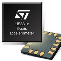
LIS3LV02DL STMicroelectronics, LIS3LV02DL Datasheet - Page 25

LIS3LV02DL
Manufacturer Part Number
LIS3LV02DL
Description
Board Mount Accelerometers MEMS INERTIAL SENSOR
Manufacturer
STMicroelectronics
Datasheet
1.LIS3LV02DL.pdf
(48 pages)
Specifications of LIS3LV02DL
Sensing Axis
X, Y, Z
Acceleration
2 g, 6 g
Digital Output - Number Of Bits
12 bit, 16 bit
Supply Voltage (max)
3.6 V
Supply Voltage (min)
2.16 V
Supply Current
0.65 mA
Maximum Operating Temperature
+ 85 C
Minimum Operating Temperature
- 40 C
Digital Output - Bus Interface
I2C, SPI
Sensitivity
1024 LSB/g
Package / Case
LGA-16
Output Type
Digital
Acceleration Range
±2g, ±6g
No. Of Axes
3
Interface Type
I2C, SPI
Sensitivity Per Axis
1024LSB / G
Sensor Case Style
LGA
No. Of Pins
16
Supply Voltage Range
2.16V To 3.6V
Rohs Compliant
Yes
Lead Free Status / RoHS Status
Lead free / RoHS Compliant
Available stocks
Company
Part Number
Manufacturer
Quantity
Price
Part Number:
LIS3LV02DL
Manufacturer:
ST
Quantity:
20 000
LIS3LV02DL
5.2.1
bit 0: RW bit. When 0, the data DI(7:0) is written into the device. When 1, the data DO(7:0)
from the device is read. In latter case, the chip will drive SDO at the start of bit 8.
bit 1: MS bit. When 0, the address will remain unchanged in multiple read/write commands.
When 1, the address will be auto incremented in multiple read/write commands.
bit 2-7: address AD(5:0). This is the address field of the indexed register.
bit 8-15: data DI(7:0) (write mode). This is the data that will be written into the device (MSb
first).
bit 8-15: data DO(7:0) (read mode). This is the data that will be read from the device (MSb
first).
In multiple read/write commands further blocks of 8 clock periods will be added. When MS
bit is 0 the address used to read/write data remains the same for every block. When MS bit
is ‘1’ the address used to read/write data is incremented at every block.
The function and the behavior of SDI and SDO remain unchanged.
SPI read
Figure 7.
The SPI Read command is performed with 16 clock pulses. Multiple byte read command is
performed adding blocks of 8 clock pulses at the previous one.
bit 0: READ bit. The value is 1.
bit 1: MS bit. When 0 do not increment address, when 1 increment address in multiple
reading.
bit 2-7: address AD(5:0). This is the address field of the indexed register.
bit 8-15: data DO(7:0) (read mode). This is the data that will be read from the device (MSb
first).
bit 16-... : data DO(...-8). Further data in multiple byte reading.
SPI read protocol
SDO
SPC
SDI
CS
RW
MS
AD5 AD4 AD3 AD2 AD1 AD0
DO7 DO6 DO5 DO4 DO3 DO2 DO1 DO0
Digital interfaces
25/48


