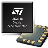
LIS3LV02DL STMicroelectronics, LIS3LV02DL Datasheet - Page 33

LIS3LV02DL
Manufacturer Part Number
LIS3LV02DL
Description
Board Mount Accelerometers MEMS INERTIAL SENSOR
Manufacturer
STMicroelectronics
Datasheet
1.LIS3LV02DL.pdf
(48 pages)
Specifications of LIS3LV02DL
Sensing Axis
X, Y, Z
Acceleration
2 g, 6 g
Digital Output - Number Of Bits
12 bit, 16 bit
Supply Voltage (max)
3.6 V
Supply Voltage (min)
2.16 V
Supply Current
0.65 mA
Maximum Operating Temperature
+ 85 C
Minimum Operating Temperature
- 40 C
Digital Output - Bus Interface
I2C, SPI
Sensitivity
1024 LSB/g
Package / Case
LGA-16
Output Type
Digital
Acceleration Range
±2g, ±6g
No. Of Axes
3
Interface Type
I2C, SPI
Sensitivity Per Axis
1024LSB / G
Sensor Case Style
LGA
No. Of Pins
16
Supply Voltage Range
2.16V To 3.6V
Rohs Compliant
Yes
Lead Free Status / RoHS Status
Lead free / RoHS Compliant
Available stocks
Company
Part Number
Manufacturer
Quantity
Price
Part Number:
LIS3LV02DL
Manufacturer:
ST
Quantity:
20 000
LIS3LV02DL
Table 33.
FS bit is used to select Full Scale value. After the device power-up the default full scale
value is +/-2g. In order to obtain a +/-6g full scale it is necessary to set FS bit to ‘1’.
BDU bit is used to inhibit output registers update between the reading of upper and lower
register parts. In default mode (BDU = ‘0’) the lower and upper register parts are updated
continuously. If it is not sure to read faster than output data rate, it is recommended to set
BDU bit to ‘1’. In this way, after the reading of the lower (upper) register part, the content of
that output registers is not updated until the upper (lower) part is read too.
This feature avoids reading LSB and MSB related to different samples.
BLE bit is used to select Big Endian or Little Endian representation for output registers. In
Big Endian’s one MSB acceleration value is located at addresses 28h (X-axis), 2Ah (Y-axis)
and 2Ch (Z-axis) while LSB acceleration value is located at addresses 29h (X-axis), 2Bh (Y-
axis) and 2Dh (Z-axis). In Little Endian representation (Default, BLE=‘0‘) the order is
inverted (refer to data register description for more details).
BOOT bit is used to refresh the content of internal registers stored in the flash memory
block. At the device power up the content of the flash memory block is transferred to the
internal registers related to trimming functions to permit a good behavior of the device itself.
If for any reason the content of trimming registers was changed it is sufficient to use this bit
to restore correct values. When BOOT bit is set to ‘1’ the content of internal flash is copied
inside corresponding internal registers and it is used to calibrate the device. These values
are factory trimmed and they are different for every accelerometer. They permit a good
behavior of the device and normally they have not to be changed. At the end of the boot
process the BOOT bit is set again to ‘0’.
IEN bit is used to switch the value present on data-ready pad between Data-Ready signal
and Interrupt signal. At power up the Data-ready signal is chosen. It is however necessary to
modify DRDY bit to enable Data-Ready signal generation.
DRDY bit is used to enable Data-Ready (RDY/INT) pin activation. If DRDY bit is ‘0’ (default
value) on Data-Ready pad a ‘0’ value is present. If a Data-Ready signal is desired it is
necessary to set to ‘1’ DRDY bit. Data-Ready signal goes to ‘1’ whenever a new data is
available for all the enabled axis. For example if Z-axis is disabled, Data-Ready signal goes
to ‘1’ when new values are available for both X and Y axis. Data-Ready signal comes back
to ‘0’ when all the registers containing values of the enabled axis are read. To be sure not to
loose any data coming from the accelerometer data registers must be read before a new
Data-Ready rising edge is generated. In this case Data-ready signal will have the same
frequency of the data rate chosen.
SIM bit selects the SPI Serial Interface Mode. When SIM is ‘0’ (default value) the 4-wire
interface mode is selected. The data coming from the device are sent to SDO pad. In 3-wire
interface mode output data are sent to SDA/SDI pad.
DAS bit permits to decide between 12 bit right justified and 16 bit left justified representation
of data coming from the device. The first case is the default case and the most significant
bits are replaced by the bit representing the sign.
SIM
DAS
Register description (continued) (21h)
SPI Serial Interface Mode selection
(0: 4-wire interface; 1: 3-wire interface)
Data Alignment Selection
(0: 12 bit right justified; 1: 16 bit left justified)
Register description
33/48


