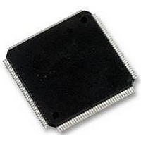
LPC2220FBD144 NXP Semiconductors, LPC2220FBD144 Datasheet - Page 13

LPC2220FBD144
Manufacturer Part Number
LPC2220FBD144
Description
IC, 16/32BIT ARM7 MCU, 64K RAM, SMD
Manufacturer
NXP Semiconductors
Datasheet
1.LPC2220FBD144.pdf
(50 pages)
Specifications of LPC2220FBD144
No. Of I/o's
76
Ram Memory Size
64KB
Cpu Speed
75MHz
No. Of Timers
2
No. Of Pwm Channels
6
Digital Ic Case Style
LQFP
Supply Voltage
RoHS Compliant
Core Size
32bit
Oscillator Type
External Only
Controller Family/series
LPC22xx
Peripherals
ADC, RTC
Rohs Compliant
Yes
Available stocks
Company
Part Number
Manufacturer
Quantity
Price
Company:
Part Number:
LPC2220FBD144
Manufacturer:
NXP
Quantity:
5 000
Company:
Part Number:
LPC2220FBD144
Manufacturer:
NXP
Quantity:
530
Part Number:
LPC2220FBD144
Manufacturer:
NXP/恩智浦
Quantity:
20 000
Company:
Part Number:
LPC2220FBD144,551
Manufacturer:
Microchip
Quantity:
150
Company:
Part Number:
LPC2220FBD144,551
Manufacturer:
NXP Semiconductors
Quantity:
10 000
Part Number:
LPC2220FBD144,551
Manufacturer:
NXP/恩智浦
Quantity:
20 000
Company:
Part Number:
LPC2220FBD144/01
Manufacturer:
FSC
Quantity:
30
NXP Semiconductors
Table 4.
LPC2210_2220_6
Product data sheet
Symbol
P3.19/A19
P3.20/A20
P3.21/A21
P3.22/A22
P3.23/A23/
XCLK
P3.24/CS3
P3.25/CS2
P3.26/CS1
P3.27/WE
P3.28/BLS3/
AIN7
P3.29/BLS2/
AIN6
P3.30/BLS1
P3.31/BLS0
n.c.
RESET
XTAL1
XTAL2
V
V
V
V
SS
SSA
SSA(PLL)
DD(1V8)
Pin description
Pin (LQFP)
46
45
44
41
40
36
35
30
29
28
27
97
96
22
135
142
141
3, 9, 26, 38,
54, 67, 79,
93, 103, 107,
111, 128
139
138
37, 110
[5]
[5]
[5]
[5]
[5]
[5]
[5]
[5]
[5]
[2]
[4]
[4]
[4]
[5]
[6]
[7]
[7]
…continued
Pin (TFBGA) Type
L5
K5
N4
K4
N3
M2
M1
K2
K1
J4
J3
E13
F10
H2
C5
C3
B3
C2, E4, J2,
N2, N7, L10,
K12, F13,
D11, B13,
B11, D7
C4
B4
N1, A12
[2]
[4]
[5]
[5]
[5]
[5]
[5]
[7]
[5]
[5]
[5]
[6]
[7]
[5]
[5]
[4]
[4]
Rev. 06 — 11 December 2008
O
O
O
O
O
O
O
O
O
O
O
I
O
I
O
O
I
I
O
I
I
I
I
Description
A19 — External memory address line 19.
A20 — External memory address line 20.
A21 — External memory address line 21.
A22 — External memory address line 22.
A23 — External memory address line 23.
XCLK — Clock output.
CS3 — LOW-active Chip Select 3 signal.
(Bank 3 addresses range 0x8300 0000 to 0x83FF FFFF)
CS2 — LOW-active Chip Select 2 signal.
(Bank 2 addresses range 0x8200 0000 to 0x82FF FFFF)
CS1 — LOW-active Chip Select 1 signal.
(Bank 1 addresses range 0x8100 0000 to 0x81FF FFFF)
WE — LOW-active Write enable signal.
BLS3 — LOW-active Byte Lane Select signal (Bank 3).
AIN7 — ADC, input 7. This analog input is always connected
to its pin.
BLS2 — LOW-active Byte Lane Select signal (Bank 2).
AIN6 — ADC, input 6. This analog input is always connected
to its pin.
BLS1 — LOW-active Byte Lane Select signal (Bank 1).
BLS0 — LOW-active Byte Lane Select signal (Bank 0).
Not connected. This pin MUST NOT be pulled LOW or the
device might not operate properly.
External reset input: A LOW on this pin resets the device,
causing I/O ports and peripherals to take on their default
states, and processor execution to begin at address 0. TTL
with hysteresis, 5 V tolerant.
Input to the oscillator circuit and internal clock generator
circuits.
Output from the oscillator amplifier.
Ground: 0 V reference.
Analog ground: 0 V reference. This should nominally be the
same voltage as V
and error.
PLL analog ground: 0 V reference. This should nominally be
the same voltage as V
noise and error.
1.8 V core power supply: This is the power supply voltage
for internal circuitry.
SS
, but should be isolated to minimize noise
SS
, but should be isolated to minimize
16/32-bit ARM microcontrollers
LPC2210/2220
© NXP B.V. 2008. All rights reserved.
13 of 50


