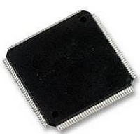
LPC2220FBD144 NXP Semiconductors, LPC2220FBD144 Datasheet - Page 22

LPC2220FBD144
Manufacturer Part Number
LPC2220FBD144
Description
IC, 16/32BIT ARM7 MCU, 64K RAM, SMD
Manufacturer
NXP Semiconductors
Datasheet
1.LPC2220FBD144.pdf
(50 pages)
Specifications of LPC2220FBD144
No. Of I/o's
76
Ram Memory Size
64KB
Cpu Speed
75MHz
No. Of Timers
2
No. Of Pwm Channels
6
Digital Ic Case Style
LQFP
Supply Voltage
RoHS Compliant
Core Size
32bit
Oscillator Type
External Only
Controller Family/series
LPC22xx
Peripherals
ADC, RTC
Rohs Compliant
Yes
Available stocks
Company
Part Number
Manufacturer
Quantity
Price
Company:
Part Number:
LPC2220FBD144
Manufacturer:
NXP
Quantity:
5 000
Company:
Part Number:
LPC2220FBD144
Manufacturer:
NXP
Quantity:
530
Part Number:
LPC2220FBD144
Manufacturer:
NXP/恩智浦
Quantity:
20 000
Company:
Part Number:
LPC2220FBD144,551
Manufacturer:
Microchip
Quantity:
150
Company:
Part Number:
LPC2220FBD144,551
Manufacturer:
NXP Semiconductors
Quantity:
10 000
Part Number:
LPC2220FBD144,551
Manufacturer:
NXP/恩智浦
Quantity:
20 000
Company:
Part Number:
LPC2220FBD144/01
Manufacturer:
FSC
Quantity:
30
NXP Semiconductors
Table 9.
LPC2210_2220_6
Product data sheet
PINSEL2 bits
1:0
2
3
5:4
6
7
8
10:9
11
12
13
15:14
17:16
19:18
20
21
22
Pin function select register 2 (PINSEL2 - 0xE002 C014)
6.8 Pin function select register 2 (PINSEL2 - 0xE002 C014)
Description
reserved
When 0, pins P1[36:26] are used as GPIO pins. When 1, P1[31:26] are used as a
Debug port.
When 0, pins P1[25:16] are used as GPIO pins. When 1, P1[25:16] are used as a
Trace port.
Controls the use of the data bus and strobe pins:
Pins P2[7:0]
Pin P1.0
Pin P1.1
Pin P3.31
Pins P2[15:8]
Pin P3.30
Pins P2[27:16]
Pins P2[29:28]
Pins P2[31:30]
Pins P3[29:28]
If bits 5:4 are not 10, controls the use of pin P3.29: 0 enables P3.29, 1 enables
AIN6.
If bits 5:4 are not 10, controls the use of pin P3.28: 0 enables P3.28, 1 enables
AIN7.
Controls the use of pin P3.27: 0 enables P3.27, 1 enables WE.
reserved
Controls the use of pin P3.26: 0 enables P3.26, 1 enables CS1.
reserved
If bits 27:25 are not 111, controls the use of pin P3.23/A23/XCLK: 0 enables P3.23,
1 enables XCLK.
Controls the use of pin P3.25: 00 enables P3.25, 01 enables CS2, 10 and 11 are
reserved values.
Controls the use of pin P3.24: 00 enables P3.24, 01 enables CS3, 10 and 11 are
reserved values.
reserved
If bits 5:4 are not 10, controls the use of pin P2[29:28]: 0 enables P2[29:28], 1 is
reserved
If bits 5:4 are not 10, controls the use of pin P2.30: 0 enables P2.30, 1 enables
AIN4.
If bits 5:4 are not 10, controls the use of pin P2.31: 0 enables P2.31, 1 enables
AIN5.
The PINSEL2 register controls the functions of the pins as per the settings listed in
Table
function is selected for a pin. For other functions direction is controlled automatically.
Settings other than those shown in
9. The direction control bit in the IODIR register is effective only when the GPIO
00 or 11 = P2[15:8]
00 or 11 = P3.30
0x or 11 = P2[27:16]
0x or 11 = P2[29:28]
0x or 11 = P2[31:30] or AIN5 to
0x or 11 = P3[29:28] or AIN7 to
11 = P2[7:0]
11 = P1.0
11 = P1.1
11 = P3.31
Rev. 06 — 11 December 2008
AIN4
AIN6
Table 9
are reserved, and should not be used.
01 or 10 = D15 to D8
01 or 10 = BLS1
0x or 10 = D7 to D0
0x or 10 = CS0
0x or 10 = OE
0x or 10 = BLS0
10 = D27 to D16
10 = D29, D28
10 = D31, D30
10 = BLS2, BLS3
16/32-bit ARM microcontrollers
LPC2210/2220
Reset value
-
P1.26/RTCK
P1.20/
TRACESYNC
BOOT1:0
1
1
0
-
0
-
0
00
00
-
0
1
1
© NXP B.V. 2008. All rights reserved.
22 of 50


