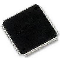
LPC2220FBD144 NXP Semiconductors, LPC2220FBD144 Datasheet - Page 23

LPC2220FBD144
Manufacturer Part Number
LPC2220FBD144
Description
IC, 16/32BIT ARM7 MCU, 64K RAM, SMD
Manufacturer
NXP Semiconductors
Datasheet
1.LPC2220FBD144.pdf
(50 pages)
Specifications of LPC2220FBD144
No. Of I/o's
76
Ram Memory Size
64KB
Cpu Speed
75MHz
No. Of Timers
2
No. Of Pwm Channels
6
Digital Ic Case Style
LQFP
Supply Voltage
RoHS Compliant
Core Size
32bit
Oscillator Type
External Only
Controller Family/series
LPC22xx
Peripherals
ADC, RTC
Rohs Compliant
Yes
Available stocks
Company
Part Number
Manufacturer
Quantity
Price
Company:
Part Number:
LPC2220FBD144
Manufacturer:
NXP
Quantity:
5 000
Company:
Part Number:
LPC2220FBD144
Manufacturer:
NXP
Quantity:
530
Part Number:
LPC2220FBD144
Manufacturer:
NXP/恩智浦
Quantity:
20 000
Company:
Part Number:
LPC2220FBD144,551
Manufacturer:
Microchip
Quantity:
150
Company:
Part Number:
LPC2220FBD144,551
Manufacturer:
NXP Semiconductors
Quantity:
10 000
Part Number:
LPC2220FBD144,551
Manufacturer:
NXP/恩智浦
Quantity:
20 000
Company:
Part Number:
LPC2220FBD144/01
Manufacturer:
FSC
Quantity:
30
NXP Semiconductors
Table 9.
LPC2210_2220_6
Product data sheet
PINSEL2 bits
23
24
27:25
31:28
Pin function select register 2 (PINSEL2 - 0xE002 C014)
6.10.1 Features
6.11.1 Features
6.10 General purpose parallel I/O
6.11 10-bit ADC
6.9 External memory controller
Description
Controls whether P3.0/A0 is a port pin (0) or an address line (1).
Controls whether P3.1/A1 is a port pin (0) or an address line (1).
Controls the number of pins among P3.23/A23/XCLK and P3[22:2]/A2[22:2] that
are address lines:
000 = None
001 = A3 to A2 are address
lines.
010 = A5 to A2 are address
lines.
011 = A7 to A2 are address
lines.
reserved
The external static memory controller is a module which provides an interface between
the system bus and external (off-chip) memory devices. It provides support for up to four
independently configurable memory banks (16 MB each with byte lane enable control)
simultaneously. Each memory bank is capable of supporting SRAM, ROM, flash EPROM,
burst ROM memory, or some external I/O devices.
Each memory bank may be 8-bit, 16-bit, or 32-bit wide.
Device pins that are not connected to a specific peripheral function are controlled by the
GPIO registers. Pins may be dynamically configured as inputs or outputs. Separate
registers allow setting or clearing any number of outputs simultaneously. The value of the
output register may be read back, as well as the current state of the port pins.
The LPC2210/2220 each contain a single 10-bit successive approximation ADC with eight
multiplexed channels.
•
•
•
•
•
•
Direction control of individual bits.
Separate control of output set and clear.
All I/O default to inputs after reset.
Measurement range of 0 V to 3 V.
Capable of performing more than 400000 10-bit samples per second.
Burst conversion mode for single or multiple inputs.
Rev. 06 — 11 December 2008
100 = A11 to A2 are address lines.
101 = A15 to A2 are address lines.
110 = A19 to A2 are address lines.
111 = A23 to A2 are address lines.
…continued
16/32-bit ARM microcontrollers
LPC2210/2220
Reset value
1 if BOOT1:0 = 00
at RESET = 0,
0 otherwise
BOOT1 during
reset
000 if
BOOT1:0 = 11 at
reset, 111
otherwise
© NXP B.V. 2008. All rights reserved.
23 of 50


