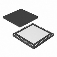
PIC24FJ256GB106-I/MR Microchip Technology, PIC24FJ256GB106-I/MR Datasheet - Page 23

PIC24FJ256GB106-I/MR
Manufacturer Part Number
PIC24FJ256GB106-I/MR
Description
IC, 16BIT MCU, PIC24F, 32MHZ, QFN-64
Manufacturer
Microchip Technology
Series
PIC® 24Fr
Datasheets
1.PIC24FJ128GA106-IPT.pdf
(52 pages)
2.PIC24FJ64GB106-IPT.pdf
(16 pages)
3.PIC24FJ64GB106-IPT.pdf
(352 pages)
4.PIC24FJ192GB108-IPT.pdf
(328 pages)
Specifications of PIC24FJ256GB106-I/MR
Controller Family/series
PIC24
No. Of I/o's
51
Ram Memory Size
16KB
Cpu Speed
32MHz
No. Of Timers
5
Core Size
16 Bit
Program Memory Size
256KB
Peripherals
ADC, Comparator, PWM, RTC, Timer
Core Processor
PIC
Speed
32MHz
Connectivity
I²C, SPI, UART/USART, USB OTG
Number Of I /o
51
Program Memory Type
FLASH
Ram Size
16K x 8
Voltage - Supply (vcc/vdd)
2 V ~ 3.6 V
Data Converters
A/D 16x10b
Oscillator Type
Internal
Operating Temperature
-40°C ~ 85°C
Package / Case
64-VFQFN, Exposed Pad
Processor Series
PIC24FJ
Core
PIC
Data Bus Width
16 bit
Data Ram Size
16 KB
Interface Type
I2C, SPI, UART
Maximum Clock Frequency
32 MHz
Number Of Programmable I/os
52
Number Of Timers
5
Maximum Operating Temperature
+ 85 C
Mounting Style
SMD/SMT
3rd Party Development Tools
52713-733, 52714-737, 53276-922, EWDSPIC
Development Tools By Supplier
PG164130, DV164035, DV244005, DV164005, PG164120, DM240001, DM240011
Minimum Operating Temperature
- 40 C
On-chip Adc
10 bit, 16 Channel
Lead Free Status / RoHS Status
Lead free / RoHS Compliant
For Use With
876-1004 - PIC24 BREAKOUT BOARD
Eeprom Size
-
Lead Free Status / Rohs Status
Details
Available stocks
Company
Part Number
Manufacturer
Quantity
Price
Company:
Part Number:
PIC24FJ256GB106-I/MR
Manufacturer:
TI
Quantity:
1 292
3.9
The procedure for reading configuration memory is
similar to the procedure for reading code memory,
except that 16-bit data words are read (with the upper
byte read being all ‘0’s) instead of 24-bit words.
Configuration Words are read one register at a time.
TABLE 3-10:
© 2007 Microchip Technology Inc.
Step 1: Exit Reset vector.
Step 2: Initialize TBLPAG, the Read Pointer (W6) and the Write Pointer (W7) for TBLRD instruction.
Step 3: Read the Configuration register and write it to the VISI register (located at 784h), and clock out the
Step 4: Repeat Step 3 twice to read Configuration Word 2 and Configuration Word 1.
Step 5: Reset device internal PC.
Command
(Binary)
0000
0000
0000
0000
0000
0000
0000
0000
0000
0000
0000
0001
0000
0000
0000
Reading Configuration Words
VISI register using the REGOUT command.
SERIAL INSTRUCTION EXECUTION FOR READING ALL CONFIGURATION MEMORY
000000
040200
000000
200xx0
880190
2xxxx7
207847
000000
BA0BB6
000000
000000
<VISI>
000000
040200
000000
(Hex)
Data
NOP
GOTO
NOP
MOV
MOV
MOV
MOV
NOP
TBLRDL
NOP
NOP
Clock out contents of VISI register
NOP
GOTO
NOP
0x200
<CW3Address23:16>, W0
W0, TBLPAG
<CW3Address15:0>, W6
#VISI, W7
[W6++], [W7]
0x200
PIC24FJXXXGA1/GB1
Table 3-10 shows the ICSP programming details for
reading the Configuration Words. Note that the
TBLPAG register must be loaded with 00h for 64 Kbyte
and below devices and 01h for 128 Kbyte and larger
devices (the upper byte address of configuration mem-
ory), and the Read Pointer, W6, is initialized to the
lower 16 bits of the Configuration Word location.
Description
DS39907A-page 23


