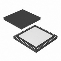
PIC24FJ256GB106-I/MR Microchip Technology, PIC24FJ256GB106-I/MR Datasheet - Page 34

PIC24FJ256GB106-I/MR
Manufacturer Part Number
PIC24FJ256GB106-I/MR
Description
IC, 16BIT MCU, PIC24F, 32MHZ, QFN-64
Manufacturer
Microchip Technology
Series
PIC® 24Fr
Datasheets
1.PIC24FJ128GA106-IPT.pdf
(52 pages)
2.PIC24FJ64GB106-IPT.pdf
(16 pages)
3.PIC24FJ64GB106-IPT.pdf
(352 pages)
4.PIC24FJ192GB108-IPT.pdf
(328 pages)
Specifications of PIC24FJ256GB106-I/MR
Controller Family/series
PIC24
No. Of I/o's
51
Ram Memory Size
16KB
Cpu Speed
32MHz
No. Of Timers
5
Core Size
16 Bit
Program Memory Size
256KB
Peripherals
ADC, Comparator, PWM, RTC, Timer
Core Processor
PIC
Speed
32MHz
Connectivity
I²C, SPI, UART/USART, USB OTG
Number Of I /o
51
Program Memory Type
FLASH
Ram Size
16K x 8
Voltage - Supply (vcc/vdd)
2 V ~ 3.6 V
Data Converters
A/D 16x10b
Oscillator Type
Internal
Operating Temperature
-40°C ~ 85°C
Package / Case
64-VFQFN, Exposed Pad
Processor Series
PIC24FJ
Core
PIC
Data Bus Width
16 bit
Data Ram Size
16 KB
Interface Type
I2C, SPI, UART
Maximum Clock Frequency
32 MHz
Number Of Programmable I/os
52
Number Of Timers
5
Maximum Operating Temperature
+ 85 C
Mounting Style
SMD/SMT
3rd Party Development Tools
52713-733, 52714-737, 53276-922, EWDSPIC
Development Tools By Supplier
PG164130, DV164035, DV244005, DV164005, PG164120, DM240001, DM240011
Minimum Operating Temperature
- 40 C
On-chip Adc
10 bit, 16 Channel
Lead Free Status / RoHS Status
Lead free / RoHS Compliant
For Use With
876-1004 - PIC24 BREAKOUT BOARD
Eeprom Size
-
Lead Free Status / Rohs Status
Details
Available stocks
Company
Part Number
Manufacturer
Quantity
Price
Company:
Part Number:
PIC24FJ256GB106-I/MR
Manufacturer:
TI
Quantity:
1 292
PIC24FJXXXGA1/GB1
5.0
5.1
The programmer and programming executive have a
master-slave relationship, where the programmer is
the master programming device and the programming
executive is the slave.
All communication is initiated by the programmer in the
form of a command. Only one command at a time can
be sent to the programming executive. In turn, the
programming executive only sends one response to
the programmer after receiving and processing a
command. The programming executive command set
is described in Section 5.2 “Programming Executive
Commands”. The response set is described in
Section 5.3 “Programming Executive Responses”.
5.1.1
The Enhanced ICSP interface is a 2-wire SPI,
implemented using the PGCx and PGDx pins. The
PGCx pin is used as a clock input pin and the clock
source must be provided by the programmer. The
PGDx pin is used for sending command data to, and
receiving response data from, the programming
executive.
Data transmits to the device must change on the rising
edge and hold on the falling edge. Data receives from
the device must change on the falling edge and hold on
the rising edge.
All data transmissions are sent to the Most Significant
bit (MSb) first, using 16-bit mode (see Figure 5-1).
FIGURE 5-1:
DS39907A-page 34
PGCx
PGDx
MSb
1
P1B
THE PROGRAMMING
EXECUTIVE
Programming Executive
Communication
P1A
14 13 12 11
COMMUNICATION INTERFACE
AND PROTOCOL
2
3
P1
4
PROGRAMMING
EXECUTIVE SERIAL
TIMING FOR DATA
RECEIVED FROM DEVICE
5
...
6
5
11
4
P2
12
3
13
2
14
P3
1
15 16
LSb
FIGURE 5-2:
Since a 2-wire SPI is used, and data transmissions are
half duplex, a simple protocol is used to control the
direction of PGDx. When the programmer completes a
command transmission, it releases the PGDx line and
allows the programming executive to drive this line
high. The programming executive keeps the PGDx line
high to indicate that it is processing the command.
After the programming executive has processed the
command, it brings PGDx low for 15 μs to indicate to the
programmer that the response is available to be clocked
out. The programmer can begin to clock out the response
23 μs after PGDx is brought low, and it must provide the
necessary amount of clock pulses to receive the entire
response from the programming executive.
After the entire response is clocked out, the program-
mer should terminate the clock on PGCx until it is time
to send another command to the programming
executive. This protocol is shown in Figure 5-3.
5.1.2
In Enhanced ICSP mode, the PIC24FJXXXGA1/GB1
devices operate from the Internal Fast RC oscillator
(FRCDIV), which has a nominal frequency of 8 MHz.
This oscillator frequency yields an effective system
clock frequency of 4 MHz. To ensure that the program-
mer does not clock too fast, it is recommended that a
4 MHz clock be provided by the programmer.
5.1.3
The programming executive uses no Watchdog Timer
or time-out for transmitting responses to the program-
mer. If the programmer does not follow the flow control
mechanism using PGCx, as described in Section 5.1.1
“Communication Interface and Protocol”, it is
possible that the programming executive will behave
unexpectedly while trying to send a response to the
programmer. Since the programming executive has no
time-out, it is imperative that the programmer correctly
follow the described communication protocol.
As a safety measure, the programmer should use the
command time-outs identified in Table 5-1. If the
command time-out expires, the programmer should
reset
programming the device again.
PGCx
PGDx
MSb
the
1
P1B
P1A
SPI RATE
TIME-OUTS
2
14 13 12 11
programming
3
P1
4
PROGRAMMING
EXECUTIVE SERIAL TIMING
FOR DATA TRANSMITTED
TO DEVICE
5
© 2007 Microchip Technology Inc.
6
...
11
executive
5
P2
12
4
13
3
14
2
P3
and
15 16
1
LSb
start


