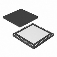
PIC24FJ256GB106-I/MR Microchip Technology, PIC24FJ256GB106-I/MR Datasheet - Page 9

PIC24FJ256GB106-I/MR
Manufacturer Part Number
PIC24FJ256GB106-I/MR
Description
IC, 16BIT MCU, PIC24F, 32MHZ, QFN-64
Manufacturer
Microchip Technology
Series
PIC® 24Fr
Datasheets
1.PIC24FJ128GA106-IPT.pdf
(52 pages)
2.PIC24FJ64GB106-IPT.pdf
(16 pages)
3.PIC24FJ64GB106-IPT.pdf
(352 pages)
4.PIC24FJ192GB108-IPT.pdf
(328 pages)
Specifications of PIC24FJ256GB106-I/MR
Controller Family/series
PIC24
No. Of I/o's
51
Ram Memory Size
16KB
Cpu Speed
32MHz
No. Of Timers
5
Core Size
16 Bit
Program Memory Size
256KB
Peripherals
ADC, Comparator, PWM, RTC, Timer
Core Processor
PIC
Speed
32MHz
Connectivity
I²C, SPI, UART/USART, USB OTG
Number Of I /o
51
Program Memory Type
FLASH
Ram Size
16K x 8
Voltage - Supply (vcc/vdd)
2 V ~ 3.6 V
Data Converters
A/D 16x10b
Oscillator Type
Internal
Operating Temperature
-40°C ~ 85°C
Package / Case
64-VFQFN, Exposed Pad
Processor Series
PIC24FJ
Core
PIC
Data Bus Width
16 bit
Data Ram Size
16 KB
Interface Type
I2C, SPI, UART
Maximum Clock Frequency
32 MHz
Number Of Programmable I/os
52
Number Of Timers
5
Maximum Operating Temperature
+ 85 C
Mounting Style
SMD/SMT
3rd Party Development Tools
52713-733, 52714-737, 53276-922, EWDSPIC
Development Tools By Supplier
PG164130, DV164035, DV244005, DV164005, PG164120, DM240001, DM240011
Minimum Operating Temperature
- 40 C
On-chip Adc
10 bit, 16 Channel
Lead Free Status / RoHS Status
Lead free / RoHS Compliant
For Use With
876-1004 - PIC24 BREAKOUT BOARD
Eeprom Size
-
Lead Free Status / Rohs Status
Details
Available stocks
Company
Part Number
Manufacturer
Quantity
Price
Company:
Part Number:
PIC24FJ256GB106-I/MR
Manufacturer:
TI
Quantity:
1 292
2.4
The program memory map extends from 000000h to
FFFFFEh. Code storage is located at the base of the
memory map and supports up to 87K instruction words
(about 256 Kbytes). Table 2-2 shows the program
memory size and number of erase and program blocks
present in each device variant. Each erase block, or
page, contains 512 instructions, and each program
block, or row, contains 64 instructions.
Locations 800000h through 8007FEh are reserved for
executive code memory. This region stores the
programming executive and the debugging executive.
The programming executive is used for device pro-
gramming and the debugging executive is used for
in-circuit debugging. This region of memory can not be
used to store user code.
TABLE 2-2:
© 2007 Microchip Technology Inc.
PIC24FJ64GB1XX
PIC24FJ128GA1XX
PIC24FJ128GB1XX
PIC24FJ192GA1XX
PIC24FJ192GB1XX
PIC24FJ256GA1XX
PIC24FJ256GB1XX
Device
Memory Map
CODE MEMORY SIZE AND FLASH CONFIGURATION WORD LOCATIONS FOR
PIC24FJXXXGA1/GB1 DEVICES
(Instruction Words)
00ABFEh (22K)
020BFEh (67K)
02ABFEh (87K)
0157FEh (44K)
Address Limit
User Memory
Blocks
Write
1048
1368
344
688
PIC24FJXXXGA1/GB1
The last three implemented program memory locations
are reserved for the Flash Configuration Words. In
PIC24FJXXXGB1 family devices, the last three loca-
tions are used for the Configuration Words; for
PIC24FJXXXGA1 devices, the last two locations are
used. The reserved addresses are shown in Table 2-2.
Locations FF0000h and FF0002h are reserved for the
Device ID registers. These bits can be used by the
programmer to identify what device type is being
programmed. They are described in Section 6.1
“Device ID”. The Device ID registers read out
normally, even after code protection is applied.
Figure 2-9
PIC24FJXXXGA1/GB1 family variants.
Blocks
Erase
131
171
43
86
shows
00ABFEh
02ABFEh
020BFEh
0157FEh
Configuration Word Addresses
1
the
memory
00ABFCh
02ABFCh
020BFCh
0157FCh
2
DS39907A-page 9
map
00ABFAh
0157FAh
020BFA
02ABFA
for
3
the


