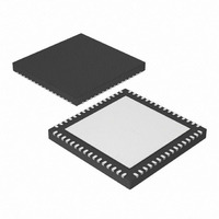
PIC24FJ256GB106-I/MR Microchip Technology, PIC24FJ256GB106-I/MR Datasheet - Page 30

PIC24FJ256GB106-I/MR
Manufacturer Part Number
PIC24FJ256GB106-I/MR
Description
IC, 16BIT MCU, PIC24F, 32MHZ, QFN-64
Manufacturer
Microchip Technology
Series
PIC® 24Fr
Datasheets
1.PIC24FJ128GA106-IPT.pdf
(52 pages)
2.PIC24FJ64GB106-IPT.pdf
(16 pages)
3.PIC24FJ64GB106-IPT.pdf
(352 pages)
4.PIC24FJ192GB108-IPT.pdf
(328 pages)
Specifications of PIC24FJ256GB106-I/MR
Controller Family/series
PIC24
No. Of I/o's
51
Ram Memory Size
16KB
Cpu Speed
32MHz
No. Of Timers
5
Core Size
16 Bit
Program Memory Size
256KB
Peripherals
ADC, Comparator, PWM, RTC, Timer
Core Processor
PIC
Speed
32MHz
Connectivity
I²C, SPI, UART/USART, USB OTG
Number Of I /o
51
Program Memory Type
FLASH
Ram Size
16K x 8
Voltage - Supply (vcc/vdd)
2 V ~ 3.6 V
Data Converters
A/D 16x10b
Oscillator Type
Internal
Operating Temperature
-40°C ~ 85°C
Package / Case
64-VFQFN, Exposed Pad
Processor Series
PIC24FJ
Core
PIC
Data Bus Width
16 bit
Data Ram Size
16 KB
Interface Type
I2C, SPI, UART
Maximum Clock Frequency
32 MHz
Number Of Programmable I/os
52
Number Of Timers
5
Maximum Operating Temperature
+ 85 C
Mounting Style
SMD/SMT
3rd Party Development Tools
52713-733, 52714-737, 53276-922, EWDSPIC
Development Tools By Supplier
PG164130, DV164035, DV244005, DV164005, PG164120, DM240001, DM240011
Minimum Operating Temperature
- 40 C
On-chip Adc
10 bit, 16 Channel
Lead Free Status / RoHS Status
Lead free / RoHS Compliant
For Use With
876-1004 - PIC24 BREAKOUT BOARD
Eeprom Size
-
Lead Free Status / Rohs Status
Details
Available stocks
Company
Part Number
Manufacturer
Quantity
Price
Company:
Part Number:
PIC24FJ256GB106-I/MR
Manufacturer:
TI
Quantity:
1 292
PIC24FJXXXGA1/GB1
TABLE 4-2:
DS39907A-page 30
I2C2SEL
ICS1:ICS0
IESO
IOL1WAY
JTAGEN
OSCIOFNC
PLLDIV2:PLLDIV0
POSCMD1:
POSCMD0
WDTPOST3:
WDTPOST0
Note 1:
Bit Field
2:
(2)
Available on PIC24FJXXXGB1XX devices only.
Available on PIC24FJXXXGA110 devices only. On other devices, always maintain this bit as ‘1’.
PIC24FJXXXGA1/GB1 CONFIGURATION BITS DESCRIPTION (CONTINUED)
(1)
CW2<14:12>
CW1<9,8>
CW2<1:0>
CW1<3:0>
CW2<15>
CW1<14>
Register
CW2<2>
CW2<4>
CW2<5>
I2C2 Pin Select bit (PIC24FJXXXGA1XX devices only)
1 = Use SCL2/SDA2 pins for I
0 = Use ASCL2/ASDA2 pins for I
ICD Emulator Pin Placement Select bits
11 = Emulator functions are shared with PGEC1/PGED1
10 = Emulator functions are shared with PGEC2/PGED2
01 = Emulator functions are shared with PGEC3/PGED3
00 = Reserved; do not use
Internal External Switchover bit
1 = Two-Speed Start-up enabled
0 = Two-Speed Start-up disabled
IOLOCK Bit One-Way Set Enable bit
0 = The OSCCON<IOLOCK> bit can be set and cleared as needed
1 = The OSCCON<IOLOCK> bit can only be set once (provided an
JTAG Enable bit
1 = JTAG enabled
0 = JTAG disabled
OSC2 Pin Function bit (except in XT and HS modes)
1 = OSC2 is clock output
0 = OSC2 is general purpose digital I/O pin
USB 96MHz PLL Prescaler Select bits
111 = Oscillator input divided by 12 (48 MHz input)
110 = Oscillator input divided by 10 (40 MHz input)
101 = Oscillator input divided by 6 (24 MHz input)
100 = Oscillator input divided by 5 (20 MHz input)
011 = Oscillator input divided by 4 (16 MHz input)
010 = Oscillator input divided by 3 (12 MHz input)
001 = Oscillator input divided by 2 (8 MHz input)
000 = Oscillator input used directly (4 MHz input)
Primary Oscillator Mode Select bits
11 = Primary oscillator disabled
10 = HS Crystal Oscillator mode
01 = XT Crystal Oscillator mode
00 = EC (External Clock) mode
Watchdog Timer Prescaler bit
1111 = 1:32,768
1110 = 1:16,384
0001 = 1:2
0000 = 1:1
.
.
.
(provided an unlocking sequence is executed)
unlocking sequence is executed). Once IOLOCK is set, this prevents
any possible future RP register changes
2
C™ module 2
Description
2
C module 2
© 2007 Microchip Technology Inc.


