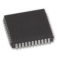
P89V51RB2FA NXP Semiconductors, P89V51RB2FA Datasheet - Page 16

P89V51RB2FA
Manufacturer Part Number
P89V51RB2FA
Description
MCU 8BIT 80C51 16K FLASH, PLCC44
Manufacturer
NXP Semiconductors
Datasheet
1.P89V51RC2FBC557.pdf
(80 pages)
Specifications of P89V51RB2FA
Controller Family/series
(8051) 8052
Core Size
8bit
No. Of I/o's
32
Program Memory Size
16KB
Ram Memory Size
1KB
Cpu Speed
40MHz
Oscillator Type
External Only
No. Of Timers
4
No. Of Pwm
RoHS Compliant
Available stocks
Company
Part Number
Manufacturer
Quantity
Price
Company:
Part Number:
P89V51RB2FA
Manufacturer:
NXP
Quantity:
1 000
Company:
Part Number:
P89V51RB2FA
Manufacturer:
NXP
Quantity:
2 000
Part Number:
P89V51RB2FA
Manufacturer:
NXP/恩智浦
Quantity:
20 000
Part Number:
P89V51RB2FA (FLA
Manufacturer:
NXP/恩智浦
Quantity:
20 000
Company:
Part Number:
P89V51RB2FA,529
Manufacturer:
NXP Semiconductors
Quantity:
10 000
Company:
Part Number:
P89V51RB2FAЈ¬529
Manufacturer:
NXP
Quantity:
150
NXP Semiconductors
Table 6.
P89V51RB2_RC2_RD2_5
Product data sheet
Reset source
External reset
Power-on reset
Watchdog reset
Brownout detect reset
Software reset
Effects of reset sources on bank selection
6.2.5 Watchdog reset
6.2.6 Data RAM memory
6.2.7 Expanded data RAM addressing
V
detection circuit will respond.
Brownout interrupt can be enabled by setting the EBO bit (IEA.3). If EBO bit is set and a
brownout condition occurs, a brownout interrupt will be generated to execute the program
at location 004BH. It is required that the EBO bit be cleared by software after the brownout
interrupt is serviced. Clearing EBO bit when the brownout condition is active will properly
reset the device. If brownout interrupt is not enabled, a brownout condition will reset the
program to resume execution at location 0000H. A brownout detect reset will clear the
BSEL bit (FCF.0) but will not change the SWR bit (FCF.1) and therefore will not change the
banking of the lower 8 kB of user code memory space.
Like a brownout detect reset, the watchdog timer reset will clear the BSEL bit (FCF.0) but
will not change the SWR bit (FCF.1) and therefore will not change the banking of the lower
8 kB of user code memory space.
The state of the SWR and BSEL bits after different types of resets is shown in
This results in the code memory bank selections as shown.
The data RAM has 1024 B of internal memory. The device can also address up to 64 kB
for external data memory.
The P89V51RB2/RC2/RD2 has 1 kB of RAM. See
memory structure” on page
The device has four sections of internal data memory:
Since the upper 128 B occupy the same addresses as the SFRs, the RAM must be
accessed indirectly. The RAM and SFRs space are physically separate even though they
have the same addresses.
1. The lower 128 B of RAM (00H to 7FH) are directly and indirectly addressable.
2. The higher 128 B of RAM (80H to FFH) are indirectly addressable.
3. The special function registers (80H to FFH) are directly addressable only.
4. The expanded RAM of 768 B (00H to 2FFH) is indirectly addressable by the move
SWR bit result
(FCF.1)
0
x
1
DD
external instruction (MOVX) and clearing the EXTRAM bit (see ‘Auxiliary function
Register’ (AUXR) in
must stay below V
BSEL bit result
(FCF.0)
0
0
0
Rev. 05 — 12 November 2009
BOD
Table 4 “Special function registers” on page
at least four oscillator clock periods before the brownout
19.
Addresses from 0000H to
1FFFH
Boot code (in block 1)
Retains state of SWR bit. If SWR,
BSEL = 00 then uses boot code.
If SWR, BSEL = 10 then uses
user code.
User code (in block 0)
P89V51RB2/RC2/RD2
8-bit microcontrollers with 80C51 core
Figure 6 “Internal and external data
Addresses above
1FFFH
User code (in block 0)
11).
© NXP B.V. 2009. All rights reserved.
Table
16 of 80
6.


