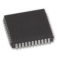
P89V51RB2FA NXP Semiconductors, P89V51RB2FA Datasheet - Page 44

P89V51RB2FA
Manufacturer Part Number
P89V51RB2FA
Description
MCU 8BIT 80C51 16K FLASH, PLCC44
Manufacturer
NXP Semiconductors
Datasheet
1.P89V51RC2FBC557.pdf
(80 pages)
Specifications of P89V51RB2FA
Controller Family/series
(8051) 8052
Core Size
8bit
No. Of I/o's
32
Program Memory Size
16KB
Ram Memory Size
1KB
Cpu Speed
40MHz
Oscillator Type
External Only
No. Of Timers
4
No. Of Pwm
RoHS Compliant
Available stocks
Company
Part Number
Manufacturer
Quantity
Price
Company:
Part Number:
P89V51RB2FA
Manufacturer:
NXP
Quantity:
1 000
Company:
Part Number:
P89V51RB2FA
Manufacturer:
NXP
Quantity:
2 000
Part Number:
P89V51RB2FA
Manufacturer:
NXP/恩智浦
Quantity:
20 000
Part Number:
P89V51RB2FA (FLA
Manufacturer:
NXP/恩智浦
Quantity:
20 000
Company:
Part Number:
P89V51RB2FA,529
Manufacturer:
NXP Semiconductors
Quantity:
10 000
Company:
Part Number:
P89V51RB2FAЈ¬529
Manufacturer:
NXP
Quantity:
150
NXP Semiconductors
P89V51RB2_RC2_RD2_5
Product data sheet
Fig 18. SPI transfer format with CPHA = 0
SPICLK (CPOL = 0)
SPICLK (CPOL = 1)
SPICLK cycle #
(for reference)
(from master)
SS (to slave)
Table 29.
Table 30.
Table 31.
Bit addressable; Reset source(s): any reset; Reset value: 0000 0000B
Table 32.
(from slave)
Bit
2
1
0
SPR1
0
0
1
1
Bit
7
6
5 to 0
Bit
Symbol
MOSI
MISO
SPCR - SPI control register (address D5H) bit description
SPCR - SPI control register (address D5H) clock rate selection
SPSR - SPI status register (address AAH) bit allocation
SPSR - SPI status register (address AAH) bit description
Symbol
CPHA
SPR1
SPR0
Symbol
SPIF
WCOL
-
SPIF
7
MSB
MSB
1
Rev. 05 — 12 November 2009
WCOL
SPR0
0
1
0
1
2
6
6
6
Description
Clock Phase control bit. 1 = shift triggered on the trailing edge of the
clock; 0 = shift triggered on the leading edge of the clock.
SPI Clock Rate Select bit 1. Along with SPR0 controls the SPICLK
rate of the device when a master. SPR1 and SPR0 have no effect on
the slave. See
SPI Clock Rate Select bit 0. Along with SPR1 controls the SPICLK
rate of the device when a master. SPR1 and SPR0 have no effect on
the slave. See
Description
SPI interrupt flag. Upon completion of data transfer, this bit is set to ‘1’.
If SPIE = 1 and ES = 1, an interrupt is then generated. This bit is
cleared by software.
Write Collision Flag. Set if the SPI data register is written to during
data transfer. This bit is cleared by software.
Reserved for future use. Should be set to ‘0’ by user programs.
3
5
5
5
-
4
4
4
Table 30
Table 30
5
3
3
P89V51RB2/RC2/RD2
4
-
SPICLK = f
4
16
64
128
below.
below.
6
2
2
8-bit microcontrollers with 80C51 core
7
1
1
3
-
osc
LSB
LSB
8
divided by
2
-
002aaa529
…continued
© NXP B.V. 2009. All rights reserved.
1
-
44 of 80
0
-


