P89V51RB2FA NXP Semiconductors, P89V51RB2FA Datasheet - Page 8
P89V51RB2FA
Manufacturer Part Number
P89V51RB2FA
Description
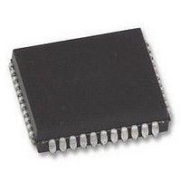
MCU 8BIT 80C51 16K FLASH, PLCC44
Manufacturer
NXP Semiconductors
Datasheet
1.P89V51RC2FBC557.pdf
(80 pages)
Specifications of P89V51RB2FA
Controller Family/series
(8051) 8052
Core Size
8bit
No. Of I/o's
32
Program Memory Size
16KB
Ram Memory Size
1KB
Cpu Speed
40MHz
Oscillator Type
External Only
No. Of Timers
4
No. Of Pwm
RoHS Compliant
Available stocks
Company
Part Number
Manufacturer
Quantity
Price
Company:

Part Number:
P89V51RB2FA
Manufacturer:
NXP
Quantity:
1 000
Company:
Part Number:
P89V51RB2FA
Manufacturer:
NXP
Quantity:
2 000
Part Number:
P89V51RB2FA
Manufacturer:
NXP/恩智浦
Quantity:
20 000
Part Number:
P89V51RB2FA (FLA
Manufacturer:
NXP/恩智浦
Quantity:
20 000
Company:
Part Number:
P89V51RB2FA,529
Manufacturer:
NXP Semiconductors
Quantity:
10 000
Company:
Part Number:
P89V51RB2FAЈ¬529
Manufacturer:
NXP
Quantity:
150


NXP Semiconductors
Table 3.
P89V51RB2_RC2_RD2_5
Product data sheet
Symbol
P2.5/A13
P2.6/A14
P2.7/A15
P3.0 to P3.7
P3.0/RXD
P3.1/TXD
P3.2/INT0
P3.3/INT1
P3.4/T0
P3.5/T1
P3.6/WR
P3.7/RD
PSEN
P89V51RB2/RC2/RD2 pin description
Pin
DIP40
26
27
28
10
11
12
13
14
15
16
17
29
TQFP44
23
24
25
5
7
8
9
10
11
12
13
26
PLCC44
29
30
31
11
13
14
15
16
17
18
19
32
Rev. 05 — 12 November 2009
…continued
Type
I/O
O
I/O
O
I/O
O
I/O with
internal
pull-up
I
I
O
O
I
I
I
I
I/O
I
I/O
I
O
O
O
O
I/O
Description
P2.5 — Port 2 bit 5.
A13 — Address bit 13.
P2.6 — Port 2 bit 6.
A14 — Address bit 14.
P2.7 — Port 2 bit 7.
A15 — Address bit 15.
Port 3: Port 3 is an 8-bit bidirectional I/O port with internal
pull-ups. Port 3 pins are pulled HIGH by the internal
pull-ups when ‘1’s are written to them and can be used as
inputs in this state. As inputs, Port 3 pins that are
externally pulled LOW will source current (I
the internal pull-ups. Port 3 also receives some control
signals and a partial of high-order address bits during the
external host mode programming and verification.
P3.0 — Port 3 bit 0.
RXD — Serial input port.
P3.1 — Port 3 bit 1.
TXD — Serial output port.
P3.2 — Port 3 bit 2.
INT0 — External interrupt 0 input.
P3.3 — Port 3 bit 3.
INT1 — External interrupt 1 input.
P3.4 — Port 3 bit 4.
T0 — External count input to Timer/counter 0.
P3.5 — Port 3 bit 5.
T1 — External count input to Timer/counter 1.
P3.6 — Port 3 bit 6.
WR — External data memory write strobe.
P3.7 — Port 3 bit 7.
RD — External data memory read strobe.
Program Store Enable: PSEN is the read strobe for
external program memory. When the device is executing
from internal program memory, PSEN is inactive (HIGH).
When the device is executing code from external program
memory, PSEN is activated twice each machine cycle,
except that two PSEN activations are skipped during each
access to external data memory. A forced HIGH-to-LOW
input transition on the PSEN pin while the RST input is
continually held HIGH for more than 10 machine cycles will
cause the device to enter external host mode
programming.
P89V51RB2/RC2/RD2
8-bit microcontrollers with 80C51 core
© NXP B.V. 2009. All rights reserved.
IL
) because of
8 of 80
Related parts for P89V51RB2FA
Image
Part Number
Description
Manufacturer
Datasheet
Request
R

Part Number:
Description:
NXP Semiconductors designed the LPC2420/2460 microcontroller around a 16-bit/32-bitARM7TDMI-S CPU core with real-time debug interfaces that include both JTAG andembedded trace
Manufacturer:
NXP Semiconductors
Datasheet:

Part Number:
Description:
NXP Semiconductors designed the LPC2458 microcontroller around a 16-bit/32-bitARM7TDMI-S CPU core with real-time debug interfaces that include both JTAG andembedded trace
Manufacturer:
NXP Semiconductors
Datasheet:
Part Number:
Description:
NXP Semiconductors designed the LPC2468 microcontroller around a 16-bit/32-bitARM7TDMI-S CPU core with real-time debug interfaces that include both JTAG andembedded trace
Manufacturer:
NXP Semiconductors
Datasheet:
Part Number:
Description:
NXP Semiconductors designed the LPC2470 microcontroller, powered by theARM7TDMI-S core, to be a highly integrated microcontroller for a wide range ofapplications that require advanced communications and high quality graphic displays
Manufacturer:
NXP Semiconductors
Datasheet:
Part Number:
Description:
NXP Semiconductors designed the LPC2478 microcontroller, powered by theARM7TDMI-S core, to be a highly integrated microcontroller for a wide range ofapplications that require advanced communications and high quality graphic displays
Manufacturer:
NXP Semiconductors
Datasheet:
Part Number:
Description:
The Philips Semiconductors XA (eXtended Architecture) family of 16-bit single-chip microcontrollers is powerful enough to easily handle the requirements of high performance embedded applications, yet inexpensive enough to compete in the market for hi
Manufacturer:
NXP Semiconductors
Datasheet:
Part Number:
Description:
The XA-S3 device is a member of Philips Semiconductors? XA(eXtended Architecture) family of high performance 16-bitsingle-chip microcontrollers
Manufacturer:
NXP Semiconductors
Datasheet:

Part Number:
Description:
The NXP BlueStreak LH75401/LH75411 family consists of two low-cost 16/32-bit System-on-Chip (SoC) devices
Manufacturer:
NXP Semiconductors
Datasheet:
Part Number:
Description:
The NXP LPC3130/3131 combine an 180 MHz ARM926EJ-S CPU core, high-speed USB2
Manufacturer:
NXP Semiconductors
Datasheet:
Part Number:
Description:
The NXP LPC3141 combine a 270 MHz ARM926EJ-S CPU core, High-speed USB 2
Manufacturer:
NXP Semiconductors
Part Number:
Description:
The NXP LPC3143 combine a 270 MHz ARM926EJ-S CPU core, High-speed USB 2
Manufacturer:
NXP Semiconductors

Part Number:
Description:
The NXP LPC3152 combines an 180 MHz ARM926EJ-S CPU core, High-speed USB 2
Manufacturer:
NXP Semiconductors
Part Number:
Description:
The NXP LPC3154 combines an 180 MHz ARM926EJ-S CPU core, High-speed USB 2
Manufacturer:
NXP Semiconductors

Part Number:
Description:
Standard level N-channel enhancement mode Field-Effect Transistor (FET) in a plastic package using NXP High-Performance Automotive (HPA) TrenchMOS technology
Manufacturer:
NXP Semiconductors
Datasheet: