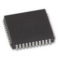
P89V51RB2FA NXP Semiconductors, P89V51RB2FA Datasheet - Page 39

P89V51RB2FA
Manufacturer Part Number
P89V51RB2FA
Description
MCU 8BIT 80C51 16K FLASH, PLCC44
Manufacturer
NXP Semiconductors
Datasheet
1.P89V51RC2FBC557.pdf
(80 pages)
Specifications of P89V51RB2FA
Controller Family/series
(8051) 8052
Core Size
8bit
No. Of I/o's
32
Program Memory Size
16KB
Ram Memory Size
1KB
Cpu Speed
40MHz
Oscillator Type
External Only
No. Of Timers
4
No. Of Pwm
RoHS Compliant
Available stocks
Company
Part Number
Manufacturer
Quantity
Price
Company:
Part Number:
P89V51RB2FA
Manufacturer:
NXP
Quantity:
1 000
Company:
Part Number:
P89V51RB2FA
Manufacturer:
NXP
Quantity:
2 000
Part Number:
P89V51RB2FA
Manufacturer:
NXP/恩智浦
Quantity:
20 000
Part Number:
P89V51RB2FA (FLA
Manufacturer:
NXP/恩智浦
Quantity:
20 000
Company:
Part Number:
P89V51RB2FA,529
Manufacturer:
NXP Semiconductors
Quantity:
10 000
Company:
Part Number:
P89V51RB2FAЈ¬529
Manufacturer:
NXP
Quantity:
150
NXP Semiconductors
P89V51RB2_RC2_RD2_5
Product data sheet
6.6.5 Framing error
6.6.6 More about UART mode 1
6.6.7 More about UART modes 2 and 3
Table 26.
Table 27.
Framing error (FE) is reported in the SCON.7 bit if SMOD0 (PCON.6) = 1. If SMOD0 = 0,
SCON.7 is the SM0 bit for the UART, it is recommended that SM0 is set up before SMOD0
is set to ‘1’.
Reception is initiated by a detected 1-to-0 transition at RXD. For this purpose RXD is
sampled at a rate of 16 times whatever baud rate has been established. When a transition
is detected, the divide-by-16 counter is immediately reset to align its rollovers with the
boundaries of the incoming bit times.
The 16 states of the counter divide each bit time into 16ths. At the 7th, 8th, and 9th
counter states of each bit time, the bit detector samples the value of RXD. The value
accepted is the value that was seen in at least 2 of the 3 samples. This is done for noise
rejection. If the value accepted during the first bit time is not 0, the receive circuits are
reset and the unit goes back to looking for another 1-to-0 transition. This is to provide
rejection of false start bits. If the start bit proves valid, it is shifted into the input shift
register, and reception of the rest of the frame will proceed.
The signal to load SBUF and RB8, and to set RI, will be generated if, and only if, the
following conditions are met at the time the final shift pulse is generated: (a) RI = 0, and
(b) either SM2 = 0, or the received stop bit = 1.
If either of these two conditions is not met, the received frame is irretrievably lost. If both
conditions are met, the stop bit goes into RB8, the 8 data bits go into SBUF, and RI is
activated.
Reception is performed in the same manner as in mode 1.
Bit
2
1
0
SM0, SM1
0 0
0 1
1 0
1 1
SCON - Serial port control register (address 98H) bit description
SCON - Serial port control register (address 98H) SM0/SM1 mode definition
Symbol
RB8
TI
RI
UART mode
0: shift register
1: 8-bit UART
2: 9-bit UART
3: 9-bit UART
Rev. 05 — 12 November 2009
Description
In modes 2 and 3, is the 9th data bit that was received. In mode 1, if
SM2 = 0, RB8 is the stop bit that was received. In mode 0, RB8 is
undefined.
Transmit interrupt flag. Set by hardware at the end of the 8th bit time in
mode 0, or at the stop bit in the other modes, in any serial
transmission. Must be cleared by software.
Receive interrupt flag. Set by hardware at the end of the 8th bit time in
mode 0, or approximately halfway through the stop bit time in all other
modes. (See SM2 for exceptions). Must be cleared by software.
P89V51RB2/RC2/RD2
8-bit microcontrollers with 80C51 core
Baud rate
CPU clock / 6
variable
CPU clock / 32 or CPU clock / 16
variable
© NXP B.V. 2009. All rights reserved.
…continued
39 of 80


