CDB3318 Cirrus Logic Inc, CDB3318 Datasheet - Page 3
CDB3318
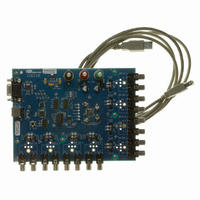
Manufacturer Part Number
CDB3318
Description
Eval Bd - 8-channel Digital Vol Cntrl
Manufacturer
Cirrus Logic Inc
Specifications of CDB3318
Main Purpose
Audio, Volume Control
Embedded
No
Utilized Ic / Part
CS3318
Primary Attributes
8 Single-Ended Analog Inputs and Outputs, USB or RS232 Interface
Secondary Attributes
Graphical User Interface
Description/function
Audio DSPs
Operating Supply Voltage
8 V to 9 V
Product
Audio Modules
Lead Free Status / RoHS Status
Contains lead / RoHS non-compliant
For Use With/related Products
CS3310
Lead Free Status / RoHS Status
Contains lead / RoHS non-compliant, Contains lead / RoHS non-compliant
Other names
598-1497


DS693F1
8. PARAMETER DEFINITIONS .............................................................................................................. 42
9. PACKAGE DIMENSIONS .................................................................................................................. 43
10. THERMAL CHARACTERISTICS AND SPECIFICATIONS ............................................................ 43
11. ORDERING INFORMATION ............................................................................................................ 44
12. REVISION HISTORY ........................................................................................................................ 44
7.5 Device Configuration 2 - Address 0Ch ........................................................................................ 34
7.6 Channel Power - Address 0Dh .................................................................................................... 35
7.7 Master Power - Address 0Eh ....................................................................................................... 35
7.8 Freeze Control - Address 0Fh ..................................................................................................... 36
7.9 Master 1 Mask - Address 10h ...................................................................................................... 36
7.10 Master 1 Volume - Address 11h ................................................................................................ 36
7.11 Master 1 Control - Address 12h ................................................................................................. 37
7.12 Master 2 Mask - Address 13h .................................................................................................... 37
7.13 Master 2 Volume - Address 14h ................................................................................................ 37
7.14 Master 2 Control - Address 15h ................................................................................................. 38
7.15 Master 3 Mask - Address 16h .................................................................................................... 38
7.16 Master 3 Volume - Address 17h ................................................................................................ 38
7.17 Master 3 Control - Address 18h ................................................................................................. 39
7.18 Group 2 Chip Address 19h ........................................................................................................ 40
7.19 Group 1 Chip Address 1Ah ........................................................................................................ 40
7.20 Individual Chip Address 1Bh ..................................................................................................... 41
7.21 Chip ID - Address 1Ch ............................................................................................................... 41
7.4.2 MUTE Input Polarity (Bit 4) ................................................................................................ 33
7.4.3 Channel B = Channel A (Bit 0 - 3) ..................................................................................... 34
7.5.1 Zero-Crossing Time-Out Period (Bits 4:2) ......................................................................... 34
7.5.2 Zero-Crossing Mode (Bits 1:0) .......................................................................................... 35
7.6.1 Power Down Channel X (Bit 0 - 7) .................................................................................... 35
7.7.1 Power Down All (Bit 0) ...................................................................................................... 35
7.8.1 Freeze (Bit 7) ..................................................................................................................... 36
7.10.1 Master 1 Volume Control (Bits 7:0) ................................................................................. 36
7.11.1 Master 1 Mute (Bit 1) ....................................................................................................... 37
7.11.2 Master 1 ¼ dB Control (Bit 0) .......................................................................................... 37
7.13.1 Master 2 Volume Control (Bits 7:0) ................................................................................. 37
7.14.1 Master 2 Mute (Bit 1) ....................................................................................................... 38
7.14.2 Master 2 ¼ dB Control (Bit 0) .......................................................................................... 38
7.16.1 Master 3 Volume Control (Bits 7:0) ................................................................................. 38
7.17.1 Master 3 Mute (Bit 1) ....................................................................................................... 39
7.17.2 Master 3 ¼ dB Control (Bit 0) .......................................................................................... 39
7.18.1 Group 2 Chip Address (Bits 7:1) ..................................................................................... 40
7.18.2 Enable Group 2 Address (Bit 0) ...................................................................................... 40
7.19.1 Group 1 Chip Address (Bits 7:1) ..................................................................................... 40
7.19.2 Enable Group 1 Address (Bit 0) ...................................................................................... 40
7.20.1 Individual Chip Address (Bits 7:1) ................................................................................... 41
7.20.2 Enable Next Device (Bit 0) .............................................................................................. 41
7.21.1 Chip ID (Bits 7:4) ............................................................................................................. 41
7.21.2 Chip Revision (Bits 3:0) ................................................................................................... 41
CS3318
3
Related parts for CDB3318
Image
Part Number
Description
Manufacturer
Datasheet
Request
R

Part Number:
Description:
Development Kit
Manufacturer:
Cirrus Logic Inc
Datasheet:
Part Number:
Description:
Development Kit
Manufacturer:
Cirrus Logic Inc
Datasheet:


Part Number:
Description:
High-efficiency PFC + Fluorescent Lamp Driver Reference Design
Manufacturer:
Cirrus Logic Inc
Datasheet:
Part Number:
Description:
Development Kit
Manufacturer:
Cirrus Logic Inc
Datasheet:
Part Number:
Description:
Development Kit
Manufacturer:
Cirrus Logic Inc
Datasheet:

Part Number:
Description:
Development Kit
Manufacturer:
Cirrus Logic Inc
Datasheet:
Part Number:
Description:
Development Kit
Manufacturer:
Cirrus Logic Inc
Datasheet:
Part Number:
Description:
Development Kit
Manufacturer:
Cirrus Logic Inc
Datasheet:
Part Number:
Description:
Development Kit
Manufacturer:
Cirrus Logic Inc
Datasheet:

Part Number:
Description:
EVALUATION BOARD FOR CS8427
Manufacturer:
Cirrus Logic Inc
Datasheet:

Part Number:
Description:
BOARD EVAL FOR CS8416 RCVR
Manufacturer:
Cirrus Logic Inc
Datasheet:

Part Number:
Description:
EVALUATION BOARD FOR CS8420
Manufacturer:
Cirrus Logic Inc
Datasheet:

Part Number:
Description:
KIT DEVELOPMENT EP9315 ARM9
Manufacturer:
Cirrus Logic Inc
Datasheet:

Part Number:
Description:
KIT DEVELOPMENT EP9302 ARM9
Manufacturer:
Cirrus Logic Inc
Datasheet: