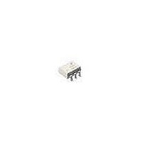
HCPL2631W Fairchild Semiconductor, HCPL2631W Datasheet - Page 3

HCPL2631W
Manufacturer Part Number
HCPL2631W
Description
High Speed Optocouplers 2Ch 10MBit/s Optocpl Logic Gate Output
Manufacturer
Fairchild Semiconductor
Datasheet
1.HCPL2631.pdf
(12 pages)
Specifications of HCPL2631W
Isolation Voltage
2500 Vrms
Maximum Continuous Output Current
50 mA
Maximum Fall Time
12 ns
Maximum Forward Diode Current
30 mA
Maximum Rise Time
50 ns
Output Device
Logic Gate Photo IC
Configuration
2 Channel
Maximum Baud Rate
10 MBps
Maximum Forward Diode Voltage
1.75 V
Maximum Reverse Diode Voltage
5 V
Maximum Power Dissipation
60 mW
Maximum Operating Temperature
+ 85 C
Minimum Operating Temperature
- 40 C
Package / Case
PDIP-8
Lead Free Status / RoHS Status
Lead free / RoHS Compliant
©2005 Fairchild Semiconductor Corporation
6N137, HCPL2601, HCPL2611, HCPL2630, HCPL2631 Rev. 1.0.8
Electrical Characteristics
Individual Component Characteristics
Switching Characteristics
EMITTER
DETECTOR
|T
Symbol
∆ V
Symbol
PHL
I
I
|CM
B
V
|CM
V
C
F
CCH
T
T
CCL
I
I
V
t
t
EH
EL
ELH
EHL
VR
EH
EL
PLH
PHL
/ ∆ T
IN
F
–T
t
t
r
f
H
L
PLH
|
|
A
| Pulse Width Distortion
Input Forward Voltage
Input Reverse Breakdown
Voltage
Input Capacitance
Input Diode Temperature
Coefficient
High Level Supply Current
Low Level Supply Current
Low Level Enable Current
High Level Enable Current
High Level Enable Voltage
Low Level Enable Voltage
Propagation Delay
Time to Output HIGH
Level
Propagation Delay
Time to Output LOW
Level
Output Rise Time
(10–90%)
Output Rise Time
(90–10%)
Enable Propagation
Delay Time to Output
HIGH Level
Enable Propagation
Delay Time to Output
LOW Level
Common Mode
Transient Immunity
(at Output HIGH Level)
Common Mode
Transient Immunity
(at Output LOW Level)
AC Characteristics
Parameter
(T
A
= -40°C to +85°C, V
(T
R
C
R
(R
R
R
I
(Fig. 13)
I
(Fig. 13)
T
(Peak), I
V
R
|V
R
V
T
|V
A
T
F
F
A
A
OH
OL
L
L
A
L
L
L
L
L
CM
CM
= 0 to 70°C unless otherwise specified)
L
= 7.5mA, V
= 7.5mA, V
I
I
V
I
V
V
Single Channel
Dual Channel
V
V
V
V
= 25°C, |V
= 25°C
= 350Ω, I
= 350 Ω ,
= 15pF
= 350 Ω , C
= 350 Ω , C
= 350 Ω , C
= 350Ω
F
R
F
= 25°C
= 350 Ω , C
F
CC
E
CC
CC
CC
CC
(Max.) = 0.8V,
(Min.) = 2.0V,
| = 400V
| = 400V
= 10mA
= 10mA
= 10µA
= 0, f = 1MHz
= 0.5V
= 5.5V, I
= 5.5V, V
= 5.5V, V
= 5.5V, I
= 5.5V, I
F
(11)
= 0mA,
(4)
(5)
(10)
F
(Fig. 12)
CM
EH
EH
L
L
L
(Fig. 14)
= 7.5mA,
L
Test Conditions
(Fig. 14)
Test Conditions
= 15pF (Fig. 12)
= 15pF
= 15pF
F
F
F
| = 50V
= 15pF (Fig. 12)
= 3.5V, R
= 3.5V, R
E
E
= 0mA,
= 10mA
= 10mA
CC
= 0.5V
= 2.0V
= 5V, I
3
(6)
(7)
T
6N137, HCPL2630
HCPL2601, HCPL2631
HCPL2611
6N137, HCPL2630
HCPL2601, HCPL2631
HCPL2611
(Fig. 12)
(Fig. 12)
(3)
L
L
A
= 350 Ω , C
= 350Ω, C
F
= 25°C
T
Single Channel
Dual Channel
V
I
V
= 7.5mA unless otherwise specified)
F
A
CC
E
= 10mA
= 25°C
= 0.5V
= 5.5V,
L
L
= 15pF
= 15pF
(8)
(9)
Min.
5.0
2.0
10,000
10,000
Min.
5000
5000
20
25
Typ.*
-1.4
-0.8
-0.6
1.4
60
10
14
10,000
10,000
15,000
10,000
10,000
15,000
7
9
Typ.*
45
45
50
12
20
20
3
Max.
1.75
-1.6
-1.6
1.8
0.8
10
15
13
21
Max. Unit
www.fairchildsemi.com
100
100
75
75
35
mV/°C
Unit
mA
mA
mA
mA
V/µs
V/µs
pF
V
V
V
V
ns
ns
ns
ns
ns
ns
ns


