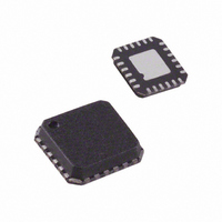
ADF4360-9BCPZ Analog Devices Inc, ADF4360-9BCPZ Datasheet - Page 21

ADF4360-9BCPZ
Manufacturer Part Number
ADF4360-9BCPZ
Description
Synthesizer And VCO
Manufacturer
Analog Devices Inc
Type
Fanout Distribution, Integer N Synthesizer (RF)r
Datasheet
1.ADF4360-9BCPZRL7.pdf
(24 pages)
Specifications of ADF4360-9BCPZ
Pll
Yes
Input
CMOS
Output
Clock
Number Of Circuits
1
Ratio - Input:output
1:2
Differential - Input:output
No/No
Frequency - Max
400MHz
Divider/multiplier
Yes/No
Voltage - Supply
3 V ~ 3.6 V
Operating Temperature
-40°C ~ 85°C
Mounting Type
Surface Mount
Package / Case
24-LFCSP
Frequency-max
400MHz
Number Of Elements
1
Supply Current
5mA
Pll Input Freq (min)
10MHz
Pll Input Freq (max)
250MHz
Operating Supply Voltage (typ)
3.3V
Operating Temp Range
-40C to 85C
Package Type
LFCSP EP
Output Frequency Range
1.1 to 400MHz
Operating Supply Voltage (min)
3V
Operating Supply Voltage (max)
3.6V
Operating Temperature Classification
Industrial
Pin Count
24
Lead Free Status / RoHS Status
Lead free / RoHS Compliant
Lead Free Status / RoHS Status
Lead free / RoHS Compliant
Available stocks
Company
Part Number
Manufacturer
Quantity
Price
Part Number:
ADF4360-9BCPZ
Manufacturer:
ADI/亚德诺
Quantity:
20 000
Company:
Part Number:
ADF4360-9BCPZRL7
Manufacturer:
Maxim
Quantity:
618
GSM TEST CLOCK
Figure 30 shows the ADF4360-9 used to generate three different
frequencies at DIVOUT. The frequencies required are 45 MHz,
80 MHz, and 95 MHz. This is achieved by generating 360 MHz,
320 MHz, and 380 MHz and programming the correct A divider
ratio. Because a 50% duty cycle is required, the A/2 DIVOUT
mode is selected. This means that A values of 4, 2, and 2 are
selected, respectively, for each of the output frequencies
previously mentioned.
The low-pass filter was designed using ADIsimPLL™ for a
channel spacing of 1 MHz and an open-loop bandwidth of
40 kHz. Larger PFD frequencies can be used to reduce in-band
noise and, therefore, rms jitter. However, for the purposes of
this example, 1 MHz is used. The measured rms jitter from this
circuit at each frequency is less than 1.5 ps.
801BE-160
20MHz
FOX
1nF
10µF
1nF
4.7kΩ
1nF
51Ω
14
16
17
18
19
12
13
CPGND
C
REF
CLK
DATA
LE
C
R
1
V
V
N
C
SET
VCO
VCO
6
IN
3
AV
8
AGND DGND L1 L2
2
DD
Figure 30.GSM Test Clock
11 22
ADF4360-9
V
Rev. A | Page 21 of 24
VDD
470Ω
DV
21
15
DD
DETECT
LOCK
9
LD
23
10
21nH
21nH
470Ω
Two 21 nH inductors are required for the specified frequency
range. The reference frequency is from a 20 MHz TCXO from
Fox; therefore, an R value of 20 is programmed. Taking into
account the high PFD frequency and its effect on the band
select logic, the band select clock divider is enabled. In this case,
a value of 8 is chosen. A very simple shunt resistor and dc-blocking
capacitor complete the RF output stage. Because these outputs
are not used, they are terminated in 50 Ω resistors. This is
recommended for circuit stability. Leaving the RF outputs
open is not recommended.
The CMOS level output frequency is available at DIVOUT. If
the frequency has to drive a low impedance load, a buffer is
recommended.
DIVOUT
RF
RF
V
OUT
OUT
TUNE
CP
B
A
24
20
7
4
5
V
VCO
51Ω
150pF
51Ω
5.6kΩ
2.2nF
12kΩ
100pF
100pF
56pF
51Ω
51Ω
ADF4360-9


