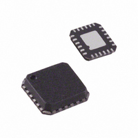
ADF4360-9BCPZ Analog Devices Inc, ADF4360-9BCPZ Datasheet - Page 23

ADF4360-9BCPZ
Manufacturer Part Number
ADF4360-9BCPZ
Description
Synthesizer And VCO
Manufacturer
Analog Devices Inc
Type
Fanout Distribution, Integer N Synthesizer (RF)r
Datasheet
1.ADF4360-9BCPZRL7.pdf
(24 pages)
Specifications of ADF4360-9BCPZ
Pll
Yes
Input
CMOS
Output
Clock
Number Of Circuits
1
Ratio - Input:output
1:2
Differential - Input:output
No/No
Frequency - Max
400MHz
Divider/multiplier
Yes/No
Voltage - Supply
3 V ~ 3.6 V
Operating Temperature
-40°C ~ 85°C
Mounting Type
Surface Mount
Package / Case
24-LFCSP
Frequency-max
400MHz
Number Of Elements
1
Supply Current
5mA
Pll Input Freq (min)
10MHz
Pll Input Freq (max)
250MHz
Operating Supply Voltage (typ)
3.3V
Operating Temp Range
-40C to 85C
Package Type
LFCSP EP
Output Frequency Range
1.1 to 400MHz
Operating Supply Voltage (min)
3V
Operating Supply Voltage (max)
3.6V
Operating Temperature Classification
Industrial
Pin Count
24
Lead Free Status / RoHS Status
Lead free / RoHS Compliant
Lead Free Status / RoHS Status
Lead free / RoHS Compliant
Available stocks
Company
Part Number
Manufacturer
Quantity
Price
Part Number:
ADF4360-9BCPZ
Manufacturer:
ADI/亚德诺
Quantity:
20 000
Company:
Part Number:
ADF4360-9BCPZRL7
Manufacturer:
Maxim
Quantity:
618
OUTPUT MATCHING
There are a number of ways to match the VCO output of the
ADF4360-9 for optimum operation; the most basic is to use a
51 Ω resistor to V
in series, as shown in Figure 33. Because the resistor is not
frequency dependent, this provides a good broadband match.
The output power in the circuit in Figure 33 typically gives
−9 dBm output power into a 50 Ω load.
A better solution is to use a shunt inductor (acting as an RF
choke) to V
output power.
Experiments have shown that the circuit shown in Figure 34
provides an excellent match to 50 Ω over the operating range of
the ADF4360-9. This gives approximately 0 dBm output power
across the specific frequency range of the ADF4360-9 using the
recommended shunt inductor, followed by a 100 pF dc-blocking
capacitor.
VCO
. This gives a better match and, therefore, more
VCO
RF
RF
Figure 34. Optimum Output Stage
V
V
Figure 33. Simple Output Stage
VCO
OUT
VCO
OUT
. A dc bypass capacitor of 100 pF is connected
51Ω
L
100pF
100pF
50Ω
50Ω
Rev. A | Page 23 of 24
The recommended value of this inductor changes with the VCO
center frequency. Figure 35 shows a graph of the optimum
inductor value vs. center frequency.
Both complementary architectures can be examined using the
EVAL-ADF4360-9EBZ1 evaluation board. If the user does not
need the differential outputs available on the ADF4360-9, the
user should either terminate the unused output with the same
circuitry as much as possible or combine both outputs using a
balun. Alternatively, instead of the LC balun, both outputs can
be combined using a 180° rat-race coupler.
If the user is only using DIVOUT and does not use the RF
outputs, it is still necessary to terminate both RF output pins
with a shunt inductor/resistor to V
capacitor and a 50 Ω load. The circuit in Figure 33 is probably
the simplest and most cost-effective solution. It is important
that the load on each pin be balanced because an unbalanced
load is likely to cause stability problems. Terminations should
be identical as much as possible.
300
250
200
150
100
Figure 35. Optimum Shunt Inductor vs. Center Frequency
50
0
0
100
CENTER FREQUENCY (MHz)
200
VCO
300
and also a dc bypass
ADF4360-9
400
500


