FDC6327C Fairchild Semiconductor, FDC6327C Datasheet
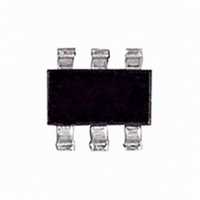
MOSFET N/P-CH DUAL 20V SSOT-6

FDC6327C

Manufacturer Part Number
FDC6327C
Description
MOSFET N/P-CH DUAL 20V SSOT-6
Manufacturer
Fairchild Semiconductor
Series
PowerTrench®r
Datasheet

Specifications of FDC6327C

Fet Type
N and P-Channel
Fet Feature
Logic Level Gate
Rds On (max) @ Id, Vgs
80 mOhm @ 2.7A, 4.5V
Drain To Source Voltage (vdss)
20V
Current - Continuous Drain (id) @ 25° C
2.7A, 1.9A
Vgs(th) (max) @ Id
1.5V @ 250µA
Gate Charge (qg) @ Vgs
4.5nC @ 4.5V
Input Capacitance (ciss) @ Vds
325pF @ 10V
Power - Max
700mW
Mounting Type
Surface Mount
Package / Case
6-SSOT, SuperSOT-6
Configuration
Dual
Transistor Polarity
N and P-Channel
Resistance Drain-source Rds (on)
0.08 Ohm @ 4.5 V @ N Channel
Forward Transconductance Gfs (max / Min)
7.7 S, 4.5 S
Drain-source Breakdown Voltage
20 V
Gate-source Breakdown Voltage
+/- 8 V
Continuous Drain Current
2.7 A @ N Channel or 1.9 A @ P Channel
Power Dissipation
960 mW
Maximum Operating Temperature
+ 150 C
Mounting Style
SMD/SMT
Minimum Operating Temperature
- 55 C
Lead Free Status / RoHS Status
Lead free / RoHS Compliant
Other names
FDC6327C
FDC6327CTR

Available stocks

Company
Part Number
Manufacturer
Quantity
Price
Part Number:
FDC6327C
Manufacturer:
FSC
Quantity:
3 000
Part Number:
FDC6327C
Manufacturer:
Fairchild Semiconductor
Quantity:
277 661
Part Number:
FDC6327C
Manufacturer:
FAIRCHILD/仙童
Quantity:
20 000
Part Number:
FDC6327C
0
Company:
Part Number:
FDC6327C
Quantity:
70 365
Company:
Part Number:
FDC6327C
Quantity:
24 000
Company:
Part Number:
FDC6327C
Quantity:
897
Part Number:
FDC6327C-NL
Manufacturer:
ON/安森美
Quantity:
20 000
Part Number:
FDC6327C_NL
Manufacturer:
FAIRCHILD/仙童
Quantity:
20 000
1999 Fairchild Semiconductor Corporation
General Description
These N & P-Channel 2.5V specified MOSFETs are
produced using Fairchild Semiconductor's advanced
PowerTrench process that has been especially tailored
to minimize on-state resistance and yet maintain low gate
charge for superior switching performance.
These devices have been designed to offer exceptional power
dissipation in a very small footprint for applications where
the bigger more expensive SO-8 and TSSOP-8 packages
are impractical.
Applications
FDC6327C
Dual N & P-Channel 2.5V Specified PowerTrench
Absolute Maximum Ratings
V
V
I
P
T
Thermal Characteristics
R
R
Package Marking and Ordering Information
Symbol
D
J
DSS
GSS
D
DC/DC converter
Load switch
Motor driving
, T
JA
JC
Device Marking
stg
SuperSOT
.327
Drain-Source Voltage
Gate-Source Voltage
Drain Current
Power Dissipation
Operating and Storage Junction Temperature Range
Thermal Resistance, Junction-to-Ambient
Thermal Resistance, Junction-to-Case
D1
S1
TM
-6
D2
- Continuous
- Pulsed
Parameter
G1
FDC6327C
Device
S2
G2
T
A
= 25°C unless otherwise noted
Reel Size
(Note 1a)
(Note 1a)
(Note 1b)
(Note 1c)
(Note 1a)
(Note 1)
Features
7”
N-Channel 2.7A, 20V. R
P-Channel -1.6A, -20V.R
Fast switching speed.
Low gate charge.
High performance trench technology for extremely
SuperSOT
low R
than SO-8); low profile (1mm thick).
DS(ON)
N-Channel
.
TM
-6 package: small footprint (72% smaller
TM
2.7
20
4
5
6
8
8
Tape Width
MOSFET
-55 to +150
8mm
R
R
0.96
130
0.9
0.7
DS(on)
60
DS(on)
DS(on)
DS(on)
P-Channel
= 0.08
= 0.25
= 0.17
= 0.12
-1.9
-20
-8
8
2
1
3
@ V
@ V
@ V
@ V
Quantity
July 2000
GS
GS
3000
GS
GS
FDC6327C, Rev. E
= 4.5V
= -4.5V
= -2.5V
= 2.5V
Units
C/W
C/W
W
V
V
A
C

Related parts for FDC6327C

FDC6327C Summary of contents

Page 1

... Device Reel Size FDC6327C 7” July 2000 TM MOSFET = 0. 4.5V DS(on 0. 2.5V DS(on 0. -4.5V DS(on 0. -2.5V DS(on package: small footprint (72% smaller P-Channel Units 20 - 2.7 -1 0.96 0.9 0.7 -55 to +150 130 60 Tape Width Quantity 8mm 3000 FDC6327C, Rev C/W C/W ...

Page 2

... P-Ch -0.4 -0.9 -1.5 N-Ch -2.1 mV/ C P-Ch 2.3 N-Ch 0.069 0.08 N-Ch 0.094 0.13 N-Ch 0.093 0.12 P-Ch 0.141 0.17 P-Ch 0.203 0.27 P-Ch 0.205 0.25 N- P-Ch -8 N-Ch 7.7 S P-Ch 4.5 N-Ch 325 pF P-Ch 315 N- P- P-Ch 24 FDC6327C, Rev. E ...

Page 3

... P-Ch (Note 140 C/W when mounted on a 0.005 in 2 pad of 2 oz. copper. Typ Max Units 3.25 4.5 nC 2.85 4.0 0.65 nC 0.68 0.90 nC 0.65 0.8 A -0.8 0.76 1.2 V -0.79 -1.2 c) 180 C/W when mounted on a 0.0015 in 2 pad of 2 oz. copper. FDC6327C, Rev. E ...

Page 4

... Gate-to-Source Voltage 125 C 1 0.1 0.01 0.001 0.0001 Figure 6. Body Diode Forward Voltage Variation with Source Current = 2.0V 2.5V 3.0V 3.5V 4. DRAIN CURRENT ( 1. 125 GATE TO SOURCE VOLTAGE ( 125 -55 C 0.4 0.8 1 BODY DIODE FORWARD VOLTAGE (V) SD and Temperature. FDC6327C, Rev 1.6 ...

Page 5

... Figure 8. Capacitance Characteristics. 5 100 0.01 0.1 100 Figure 10. Single Pulse Maximum f = 1MHz ISS C OSS C RSS DRAIN TO SOURCE VOLTAGE (V) DS SINGLE PULSE 180 C 100 1000 SINGLE PULSE TIME (SEC) Power Dissipation. FDC6327C, Rev ...

Page 6

... Gate-to-Source Voltage 125 C 0.1 0.01 0.001 0.0001 Figure 16. Body Diode Forward Voltage Variation with Source Current = -2.0V -2.5V -3.0V -3.5V -4.0V -4. DIRAIN CURRENT ( - 125 GATE TO SOURCE VOLTAGE ( 125 -55 C 0.4 0.8 1 BODY DIODE FORWARD VOLTAGE (V) SD and Temperature. FDC6327C, Rev 1.6 ...

Page 7

... Figure 18. Capacitance Characteristics. 5 100 0.01 0.1 100 Figure 20. Single Pulse Maximum MHz ISS C OSS C RSS DRAIN TO SOURCE VOLTAGE (V) DS SINGLE PULSE 180 C 100 1000 SINGLE PULSE TIME (SEC) Power Dissipation. FDC6327C, Rev ...

Page 8

... Typical Characteristics: N & P-Channel 0.5 0.5 0.2 0.2 0.1 0.1 0.05 0.05 0.02 0.01 Single Pulse 0.02 0.01 0.0001 0.001 Figure 21. Transient Thermal Response Curve. (continued) 0.01 0 TIME (sec ( 180°C/W JA P(pk ( Duty Cycle 100 300 FDC6327C, Rev. E ...

Page 9

TRADEMARKS DISCLAIMER LIFE SUPPORT POLICY PRODUCT STATUS DEFINITIONS Definition of Terms Datasheet Identification Product Status Definition ...

Related keywords