FDC6036P_F077 Fairchild Semiconductor, FDC6036P_F077 Datasheet - Page 2
FDC6036P_F077
Manufacturer Part Number
FDC6036P_F077
Description
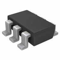
MOSFET P-CH DUAL 20V 5A 6SSOT
Manufacturer
Fairchild Semiconductor
Series
PowerTrench®r
Datasheet
1.FDC6036P_F077.pdf
(7 pages)
Specifications of FDC6036P_F077
Fet Type
2 P-Channel (Dual)
Fet Feature
Logic Level Gate
Rds On (max) @ Id, Vgs
44 mOhm @ 5A, 4.5V
Drain To Source Voltage (vdss)
20V
Current - Continuous Drain (id) @ 25° C
5A
Vgs(th) (max) @ Id
1.5V @ 250µA
Gate Charge (qg) @ Vgs
14nC @ 4.5V
Input Capacitance (ciss) @ Vds
992pF @ 10V
Power - Max
900mW
Mounting Type
Surface Mount
Package / Case
6-SSOT FLMP, SuperSOT-6 FLMP
Lead Free Status / RoHS Status
Lead free / RoHS Compliant


Electrical Characteristics
Symbol
Off Characteristics
BV
∆BV
I
I
On Characteristics
V
∆V
R
gfs
Drain–Source Diode Characteristics and Maximum Ratings
I
V
trr
Qrr
Dynamic Characteristics
C
C
C
Rg
Switching Characteristics
t
t
t
t
Q
Q
Q
DSS
GSS
S
d(on)
r
d(off)
f
GS(th)
DS(on)
SD
∆T
∆T
iss
oss
rss
g
gs
gd
DSS
GS(th)
DSS
J
J
Drain–Source BreakdownVoltage V
Breakdown Voltage Temperature
Coefficient
Zero Gate Voltage Drain Current
Gate–Body Leakage
Gate Threshold Voltage
Gate Threshold Voltage
Temperature Coefficient
Static Drain–Source
On–Resistance
Forward Transconductance
Input Capacitance
Output Capacitance
Reverse Transfer Capacitance
Gate Resistance
Turn–On Delay Time
Turn–On Rise Time
Turn–Off Delay Time
Turn–Off Fall Time
Total Gate Charge
Gate–Source Charge
Gate–Drain Charge
Maximum Continuous Drain–Source Diode Forward Current
Drain–Source Diode Forward
Voltage
Diode Reverse Recovery Time
Diode Reverse Recovery Charge
Parameter
(Note 2)
(Note 2)
I
V
V
V
I
V
V
V
V
V
V
f = 1.0 MHz
V
V
V
V
V
V
I
d
D
D
F
iF
GS
DS
GS
DS
GS
GS
GS
GS
DS
DS
DD
GS
DS
GS
GS
T
GS
= –5 A,
= –250 µA, Referenced to 25°C
= –250 µA, Referenced to 25°C
/d
A
= 25°C unless otherwise noted
= 0 V,
= –16 V,
= ±8 V,
= V
= –4.5 V,
= –2.5 V,
= –1.8 V,
= –4.5 V,I
= –5 V,
= –10 V,
= –10 V,
= –4.5 V,
= –10 V,
= –4.5 V
= 0 V,
t
= 15 mV
= 100 A/µs
Test Conditions
GS
,
I
S
D
= –1.25 A
= –5 A,T
V
f = 1.0 MHz
I
V
I
I
I
I
I
V
I
R
I
GS
D
D
D
D
D
D
D
D
DS
GS
GEN
= –250 µA
= –250 µA
= –5.0 A
= –4.0 A
= –3.2 A
= –5 A
= –1 A,
= –5 A,
= 0 V
= 0 V
= 0 V,
= 6 Ω
J
=125°C
(Note 2)
Min
–0.4
–20
Typ
–0.7
–0.7
–24
4.4
7.8
992
169
37
52
74
51
16
19
8.6
1.7
2.0
85
12
10
40
20
10
–1.25
Max
±100
–1.5
–1.2
–1
44
64
95
61
24
20
64
36
14
FDC6036P Rev C3 (W)
Units
mV/°C
mV/°C
mΩ
µA
nA
pF
pF
Ω
nC
nC
nC
nC
pF
ns
ns
ns
ns
ns
V
V
S
A
V
Related parts for FDC6036P_F077
Image
Part Number
Description
Manufacturer
Datasheet
Request
R

Part Number:
Description:
MOSFET P-CHAN DUAL 20V 5A 6SSOT
Manufacturer:
Fairchild Semiconductor
Datasheet:

Part Number:
Description:
Fdc6036p P-channel 1.8v Specified Powertrench? Mosfet
Manufacturer:
Fairchild Semiconductor
Datasheet:

Part Number:
Description:
Isolated And Regulated 60 Watt Modular Dc/dc Converters
Manufacturer:
Astrodyne Corporation
Datasheet:
Part Number:
Description:
60 WATTS OUTPUT POWER
Manufacturer:
ETC1 [List of Unclassifed Manufacturers]
Datasheet:
Part Number:
Description:
Isolated and Regulated 60 WATT Modular DC/DC Converters
Manufacturer:
ASTRODYNE [Astrodyne Corporation]
Datasheet:
Part Number:
Description:
Fairchild Semiconductor [IGBT MODULE]
Manufacturer:
Fairchild Semiconductor
Datasheet:

Part Number:
Description:
Discrete Semiconductor Modules
Manufacturer:
Fairchild Semiconductor
Part Number:
Description:
Discrete Semiconductor Modules
Manufacturer:
Fairchild Semiconductor
Part Number:
Description:
This N-Channel MOSFET is produced using Fairchild Semiconductor’s advanced Power Trench® process
Manufacturer:
Fairchild Semiconductor
Datasheet:
Part Number:
Description:
This N-Channel MOSFET is produced using Fairchild Semiconductor’s advanced Power Trench® process
Manufacturer:
Fairchild Semiconductor
Datasheet:
Part Number:
Description:
This N-Channel MOSFET is produced using Fairchild Semiconductor’s advanced PowerTrench® process
Manufacturer:
Fairchild Semiconductor
Datasheet:
Part Number:
Description:
This N-Channel MOSFET is produced using Fairchild Semiconductor’s advanced PowerTrench® process
Manufacturer:
Fairchild Semiconductor
Datasheet:
Part Number:
Description:
This N-Channel MOSFET is produced using Fairchild Semiconductor’s advanced Power Trench® process
Manufacturer:
Fairchild Semiconductor
Datasheet:
Part Number:
Description:
This N-Channel logic Level MOSFETs are produced using Fairchild Semiconductor‘s advanced Power Trench® process that has been special tailored to minimize the on-state resistance and yet maintain superior switching performance
Manufacturer:
Fairchild Semiconductor
Datasheet:
Part Number:
Description:
This N-Channel MOSFET is produced using Fairchild Semiconductor’s advanced Power Trench® process
Manufacturer:
Fairchild Semiconductor
Datasheet: