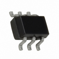
FDG6320C_D87Z Fairchild Semiconductor, FDG6320C_D87Z Datasheet - Page 6

FDG6320C_D87Z
Manufacturer Part Number
FDG6320C_D87Z
Description
MOSFET N/P-CH DUAL 25V SC70-6
Manufacturer
Fairchild Semiconductor
Specifications of FDG6320C_D87Z
Fet Type
N and P-Channel
Fet Feature
Logic Level Gate
Rds On (max) @ Id, Vgs
4 Ohm @ 220mA, 4.5V
Drain To Source Voltage (vdss)
25V
Current - Continuous Drain (id) @ 25° C
220mA, 140mA
Vgs(th) (max) @ Id
1.5V @ 250µA
Gate Charge (qg) @ Vgs
0.4nC @ 4.5V
Input Capacitance (ciss) @ Vds
9.5pF @ 10V
Power - Max
300mW
Mounting Type
Surface Mount
Package / Case
SC-70-6, SC-88, SOT-363
Lead Free Status / RoHS Status
Lead free / RoHS Compliant
Typical Electrical Characteristics: P-Channel
0.15
0.05
0.14
0.12
0.08
0.06
0.04
0.02
0.2
0.1
0.1
Figure 11. On-Region Characteristics.
Figure 13. On-Resistance Variation
Figure 15. Transfer Characteristics.
0
0
1.6
1.4
1.2
0.8
0.6
0
0
1
-50
V
DS
= -5.0V
V
I = -0.14A
D
GS
-25
V
= -4.5V
-V
GS
-V
with Temperature.
GS
1
1
DS
= -4.5V
, GATE TO SOURCE VOLTAGE (V)
T , JUNCTION TEMPERATURE (°C)
0
, DRAIN-SOURCE VOLTAGE (V)
J
-3.5V
25
T = -55°C
A
2
2
-3.0V
50
-2.7V
25°C
75
-2.5V
125°C
3
3
100
-2.0V
125
4
4
150
2.5
1.5
0.5
25
20
15
10
5
0
2
1
1.5
0.0001
0
0.001
Figure 16. Body Diode Forward Voltage
0.01
Figure 12. On-Resistance Variation with
Figure 14. On-Resistance Variation with
0.3
0.1
0.2
V
GS
V
GS
2
= -2.0V
= 0V
-V
-V
0.05
GS
SD
0.4
2.5
, GATE TO SOURCE VOLTAGE (V)
, BODY DIODE FORWARD VOLTAGE (V)
Drain Current and Gate Voltage.
Variation with Source Current
and Temperature.
-I , DRAIN CURRENT (A)
Gate-to-Source Voltage.
D
-2.5V
3
0.6
T = 125°C
A
-2.7V
0.1
3.5
25°C
-3.0V
0.8
-55°C
T = 125°C
A
T = 25°C
4
-3.5V
A
0.15
I = -0.07A
D
-4.0V
1
FDG6320C.Rev D
4.5
-4.5V
1.2
0.2
5


