FDN5630 Fairchild Semiconductor, FDN5630 Datasheet
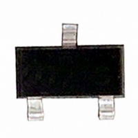
MOSFET N-CH 60V 1.7A SSOT3

FDN5630

Manufacturer Part Number
FDN5630
Description
MOSFET N-CH 60V 1.7A SSOT3
Manufacturer
Fairchild Semiconductor
Series
PowerTrench®r
Datasheet

Specifications of FDN5630

Fet Type
MOSFET N-Channel, Metal Oxide
Fet Feature
Logic Level Gate
Rds On (max) @ Id, Vgs
100 mOhm @ 1.7A, 10V
Drain To Source Voltage (vdss)
60V
Current - Continuous Drain (id) @ 25° C
1.7A
Vgs(th) (max) @ Id
3V @ 250µA
Gate Charge (qg) @ Vgs
10nC @ 10V
Input Capacitance (ciss) @ Vds
400pF @ 15V
Power - Max
460mW
Mounting Type
Surface Mount
Package / Case
3-SSOT, SuperSOT-3
Configuration
Single
Transistor Polarity
N-Channel
Resistance Drain-source Rds (on)
0.1 Ohm @ 10 V
Forward Transconductance Gfs (max / Min)
6 S
Drain-source Breakdown Voltage
60 V
Gate-source Breakdown Voltage
+/- 20 V
Continuous Drain Current
1.7 A
Power Dissipation
500 mW
Maximum Operating Temperature
+ 150 C
Mounting Style
SMD/SMT
Minimum Operating Temperature
- 55 C
Lead Free Status / RoHS Status
Lead free / RoHS Compliant
Other names
FDN5630TR

Available stocks

Company
Part Number
Manufacturer
Quantity
Price
Part Number:
FDN5630
Manufacturer:
FSC
Quantity:
36 000
Part Number:
FDN5630
Manufacturer:
Fairchild Semiconductor
Quantity:
108 793
Part Number:
FDN5630
Manufacturer:
FAIRCHILD/仙童
Quantity:
20 000
Company:
Part Number:
FDN5630
Quantity:
30 000
Part Number:
FDN5630-NL
Manufacturer:
FAIRCHILD/仙童
Quantity:
20 000
Part Number:
FDN5630_NL
Manufacturer:
FAIRCHILD/仙童
Quantity:
20 000
2000 Fairchild Semiconductor Corporation
FDN5630
60V N-Channel PowerTrench MOSFET
General Description
This N-Channel MOSFET has been designed specifically
to improve the overall efficiency of DC/DC converters using
either synchronous or conventional switching PWM
controllers.
This MOSFET features very low R
footprint. Fairchild’s PowerTrench technology provides
faster switching than other MOSFETs with comparable
R
efficiency with less board space.
Applications
Absolute Maximum Ratings
V
V
I
P
T
Thermal Characteristics
R
R
Package Marking and Ordering Information
Symbol
D
DS(ON)
J
DSS
GSS
D
DC/DC converter
Motor drives
, T
JA
JC
Device Marking
stg
specifications. The result is higher overall
SuperSOT -3
5630
Drain-Source Voltage
Gate-Source Voltage
Drain Current
Power Dissipation for Single Operation
Operating and Storage Junction Temperature Range
Thermal Resistance, Junction-to-Ambient
Thermal Resistance, Junction-to-Case
D
TM
G
- Continuous
- Pulsed
DS(ON)
Parameter
FDN5630
in a small SOT23
Device
S
T
A
= 25 C unless otherwise noted
Reel Size
Features
7
(Note 1a)
(Note 1a)
(Note 1b)
(Note 1a)
(Note 1)
1.7 A, 60 V. R
Optimized for use in high frequency DC/DC converters.
Low gate charge.
Very fast switching.
SuperSOT
TM
R
- 3 provides low R
DS(ON)
DS(ON)
G
Tape Width
-55 to +150
= 0.100
= 0.120
Ratings
8mm
D
0.46
250
1.7
0.5
60
10
75
20
@ V
@ V
DS(ON)
S
GS
GS
in SOT23 footprint.
= 10 V
= 6 V.
3000 units
Quantity
March 2000
Units
C/W
C/W
W
V
V
A
FDN5630 Rev. C
C

Related parts for FDN5630

FDN5630 Summary of contents

Page 1

... C unless otherwise noted A Parameter (Note 1a) (Note 1a) (Note 1b) (Note 1a) (Note 1) Device Reel Size FDN5630 7 March 2000 = 0.100 @ DS(ON 0.120 @ DS(ON provides low R in SOT23 footprint. DS(ON Ratings Units 1 0.5 W 0.46 -55 to +150 C 250 C/W 75 C/W Tape Width Quantity 8mm 3000 units FDN5630 Rev. C ...

Page 2

... MHz GEN 1 0.42 A (Note determined by the user's board design 270 C/W when mounted on a minimum pad. Min Typ Max Units mV 100 nA -100 6.9 mV/ C 0.073 0.100 0.127 0.180 0.083 0.120 400 pF 102 1.6 nC 1.2 nC 0.42 A 0.72 1.2 V FDN5630 Rev. C ...

Page 3

... Gate-to-Source Voltage - 125 C 1 0.1 0.01 0.001 Figure 6. Body Diode Forward Voltage Variation with Source Current = 4.5V 5.0V 6.0V 7.0V 10V DRAIN CURRENT ( 1. 125 GATE TO SOURCE VOLTAGE ( =125 -55 C 0.2 0.4 0.6 0 BODY DIODE VOLTAGE (V) SD and Temperature. FDN5630 Rev 1.2 ...

Page 4

... Thermal characterization performed using the conditions described in Note 1b. Transient themal response will change depending on the circuit board design 1MHz OSS C RSS DRAIN TO SOURCE VOLTAGE (V) DS SINGLE PULSE o R =270 C = 0.01 0 100 SINGLE PULSE TIME (SEC) Power Dissipation. R ( 270 C/W JA P(pk ( Duty Cycle 100 300 FDN5630 Rev 1000 ...

Page 5

... TRADEMARKS The following are registered and unregistered trademarks Fairchild Semiconductor owns or is authorized to use and is not intended exhaustive list of all such trademarks. ACEx™ Bottomless™ CoolFET™ CROSSVOLT™ CMOS FACT™ FACT Quiet Series™ FAST FASTr™ GTO™ ...

Related keywords