FDS2734 Fairchild Semiconductor, FDS2734 Datasheet
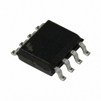
MOSFET N-CH 250V 3A 8-SOIC

FDS2734

Manufacturer Part Number
FDS2734
Description
MOSFET N-CH 250V 3A 8-SOIC
Manufacturer
Fairchild Semiconductor
Series
UltraFET™r
Datasheet

Specifications of FDS2734

Fet Type
MOSFET N-Channel, Metal Oxide
Fet Feature
Logic Level Gate
Rds On (max) @ Id, Vgs
117 mOhm @ 3A, 10V
Drain To Source Voltage (vdss)
250V
Current - Continuous Drain (id) @ 25° C
3A
Vgs(th) (max) @ Id
4V @ 250µA
Gate Charge (qg) @ Vgs
45nC @ 10V
Input Capacitance (ciss) @ Vds
2610pF @ 100V
Power - Max
1W
Mounting Type
Surface Mount
Package / Case
8-SOIC (3.9mm Width)
Configuration
Single Quad Drain Triple Source
Transistor Polarity
N-Channel
Resistance Drain-source Rds (on)
0.097 Ohms
Forward Transconductance Gfs (max / Min)
15.1 S
Drain-source Breakdown Voltage
250 V
Gate-source Breakdown Voltage
+/- 20 V
Continuous Drain Current
3 A
Power Dissipation
2.5 W
Maximum Operating Temperature
+ 150 C
Mounting Style
SMD/SMT
Minimum Operating Temperature
- 55 C
Lead Free Status / RoHS Status
Lead free / RoHS Compliant
Other names
FDS2734TR

Available stocks

Company
Part Number
Manufacturer
Quantity
Price
Part Number:
FDS2734
Manufacturer:
FSC
Quantity:
20 000
Part Number:
FDS2734-NL
Manufacturer:
FAIRCHILD
Quantity:
2 500
©2006 Fairchild Semiconductor Corporation
FDS2734 Rev. B
MOSFET Maximum Ratings
Thermal Characteristics
Package Marking and Ordering Information
V
V
I
E
P
T
R
R
R
FDS2734
N-Channel UItraFET Trench
250V, 3.0A, 117mΩ
Features
D
J
DS
GS
AS
D
θJA
θJA
θJC
Symbol
, T
Max r
Max r
Fast switching speed
High performance trench
low r
High power and current handling capability
RoHS compliant
Device Marking
STG
FDS2734
DS(on)
DS(on)
DS(on)
SO-8
Drain to Source Voltage
Gate to Source Voltage
Drain Current -Continuous
Single Pulse Avalanche Energy
Power dissipation
Power dissipation
Operating and Storage Junction Temperature Range
Thermal Resistance, Junction- to -Ambient
Thermal Resistance, Junction- to- Ambient
Thermal Resistance, Junction -to- Case
=117mΩ at V
=126mΩ at V
D
D
Pin 1
D
D
-Pulsed
GS
GS
FDS2734
=10V, I
= 6V, I
technology for
Device
S
S
D
D
= 2.8A
= 3.0A
S
Parameter
T
G
A
= 25°C unless otherwise noted
extremely
Package
SO-8
1
®
General Descriptions
This single N-Channel MOSFET is produced using
Fairchild Semiconductor’s advanced UItraFET Trench
process that has been especially tailored to minimize
the on-state resistance and yet maintain superior switching
performance.
Application
DC-DC conversion
MOSFET
Reel Size
13’’
(Note 1a)
(Note 1a)
(Note 1b)
(Note 1a)
(Note 1b)
(Note 3)
(Note 1)
5
6
7
8
Tape Width
12mm
-55 to 150
Ratings
12.5
250
±20
125
3.0
2.5
1.0
25
50
50
4
3
2
1
www.fairchildsemi.com
August 2006
2500 units
Quantity
Units
o
C/W
mJ
o
W
V
V
A
C
®
tm

Related parts for FDS2734

FDS2734 Summary of contents

Page 1

... Thermal Resistance, Junction -to- Case θJC Package Marking and Ordering Information Device Marking Device FDS2734 FDS2734 ©2006 Fairchild Semiconductor Corporation FDS2734 Rev. B ® MOSFET General Descriptions This single N-Channel MOSFET is produced using = 3.0A D Fairchild Semiconductor’s advanced UItraFET Trench process that has been especially tailored to minimize = 2 ...

Page 2

... R is guaranteed by design while R θJC a) 50°C/W when mounted on a 1in pad copper µs, 2: Pulse Test Width <300 Duty Cycle <2%. ° 3: Starting 1mH 5A 100V FDS2734 Rev 25°C unless otherwise noted J Test Conditions I = 250µ 250µA, referenced 200V ...

Page 3

... JUNCTION TEMPERATURE J Figure 3. Normalized On Resistance vs Junction Temperature 20 PULSE DURATION = 80 µ s DUTY CYCLE = 0.5%MAX 150 GATE TO SOURCE VOLTAGE (V) GS Figure 5. Transfer Characteristics FDS2734 Rev 25°C unless otherwise noted J 2.5 2.0 1.5 1.0 µ Figure 2. 0.4 0.3 0.2 0.1 0.0 75 100 125 150 3 ...

Page 4

... OPERATION IN THIS SINGLE PULSE AREA MAY MAX RATED J LIMITED DS(on DRAIN TO SOURCE VOLTAGE (V) DS Forward Bias Safe Operating Area Figure 11. FDS2734 Rev 25°C unless otherwise noted J 5000 1000 V = 125V 200V DD 100 10 0 Figure 8. 3.5 3.0 2 2.0 J 1.5 1.0 0.5 R 0.0 10 100 25 Figure 10 ...

Page 5

... SINGLE PULSE 1E Figure 13. Transient Thermal Response Curve Thermal characterization performed using the conditions described in Note 1b Transient thermal response will change depending on the circuit board design FDS2734 Rev 25°C unless otherwise noted RECTANGULAR PULSE DURATION( ...

Page 6

... TRADEMARKS The following are registered and unregistered trademarks Fairchild Semiconductor owns or is authorized to use and is not intended exhaustive list of all such trademarks. ACEx™ FACT Quiet Series™ ActiveArray™ GlobalOptoisolator™ Bottomless™ GTO™ Build it Now™ HiSeC™ ...

Related keywords