FDC655BN Fairchild Semiconductor, FDC655BN Datasheet
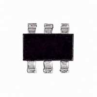
MOSFET N-CH 30V 6.3A SSOT-6

FDC655BN

Manufacturer Part Number
FDC655BN
Description
MOSFET N-CH 30V 6.3A SSOT-6
Manufacturer
Fairchild Semiconductor
Series
PowerTrench®r
Datasheet

Specifications of FDC655BN

Fet Type
MOSFET N-Channel, Metal Oxide
Fet Feature
Logic Level Gate
Rds On (max) @ Id, Vgs
25 mOhm @ 6.3A, 10V
Drain To Source Voltage (vdss)
30V
Current - Continuous Drain (id) @ 25° C
6.3A
Vgs(th) (max) @ Id
3V @ 250µA
Gate Charge (qg) @ Vgs
15nC @ 10V
Input Capacitance (ciss) @ Vds
570pF @ 15V
Power - Max
800mW
Mounting Type
Surface Mount
Package / Case
6-SSOT, SuperSOT-6
Configuration
Single Quad Drain
Transistor Polarity
N-Channel
Resistance Drain-source Rds (on)
0.025 Ohm @ 10 V
Forward Transconductance Gfs (max / Min)
20 S
Drain-source Breakdown Voltage
30 V
Gate-source Breakdown Voltage
+/- 20 V
Continuous Drain Current
6.3 A
Power Dissipation
1600 mW
Maximum Operating Temperature
+ 150 C
Mounting Style
SMD/SMT
Minimum Operating Temperature
- 55 C
Lead Free Status / RoHS Status
Lead free / RoHS Compliant
Other names
FDC655BN

Available stocks

Company
Part Number
Manufacturer
Quantity
Price
Part Number:
FDC655BN
Manufacturer:
Fairchild Semiconductor
Quantity:
168 574
Part Number:
FDC655BN
Manufacturer:
MAXIM
Quantity:
650
Part Number:
FDC655BN
Manufacturer:
FAIRCHILD
Quantity:
8 000
Part Number:
FDC655BN
Manufacturer:
FAIRCHILD/仙童
Quantity:
20 000
Part Number:
FDC655BN
0
Company:
Part Number:
FDC655BN
Quantity:
30 000
©2010 Fairchild Semiconductor Corporation
FDC655BN Rev.C2
MOSFET Maximum Ratings
Thermal Characteristics
Package Marking and Ordering Information
FDC655BN
Single N-Channel, Logic Level, PowerTrench
30 V, 6.3 A, 25 mΩ
Features
V
V
I
P
T
R
D
J
DS
GS
D
θJA
Max r
Max r
Fast switching
Low gate charge
High performance trchnology for extremely low r
Termination is Lead-free and RoHS Compliant
, T
Symbol
Device Marking
STG
DS(on)
DS(on)
.55B
= 25 mΩ at V
= 33 mΩ at V
Drain to Source Voltage
Gate to Source Voltage
Power Dissipation
Power Dissipation
Operating and Storage Junction Temperature Range
Thermal Resistance, Junction to Ambient
GS
GS
= 10 V, I
= 4.5 V, I
FDC655BN
-Continuous
-Pulsed
Device
D
D
= 6.3 A
= 5.5 A
T
C
= 25°C unless otherwise noted
DS(on)
Parameter
SSOT-6
Package
1
TM
T
General Description
This
Fairchild Semiconductor’s advanced PowerTrench
that has been especially tailored to minimize the on-state
resistance and yet maintain superior switching performance.
These devices are well suited for low voltage and battery
powered applicatoins where low in-line power loss and fast
switching are required.
A
= 25°C
D
D
G
N-Channel Logic Level MOSFET
Reel Size
7 ’’
®
( Note 1a)
(Note 1a)
(Note 1a)
(Note 1b)
MOSFET
Tape Width
8 mm
-55 to + 150
Ratings
±20
6.3
1.6
0.8
30
20
78
is produced using
January 2010
www.fairchildsemi.com
3000 units
D
S
D
Quantity
®
process
Units
°C/W
°C
W
V
V
A
tm

Related parts for FDC655BN

FDC655BN Summary of contents

Page 1

... R Thermal Resistance, Junction to Ambient θJA Package Marking and Ordering Information Device Marking Device .55B FDC655BN ©2010 Fairchild Semiconductor Corporation FDC655BN Rev.C2 General Description = 6.3 A This N-Channel Logic Level MOSFET D Fairchild Semiconductor’s advanced PowerTrench = 5 that has been especially tailored to minimize the on-state resistance and yet maintain superior switching performance ...

Page 2

... FR-4 board. b. 156 °C/W when mounted on a minimum pad. 2: Pulse Test: Pulse Width<300 us, Duty Cycle<2.0%. ©2010 Fairchild Semiconductor Corporation FDC655BN Rev. 25°C unless otherwise noted J Test Conditions = 250 µ 250 µA, referenced to 25°C ...

Page 3

... J Figure 3. Normalized On Resistance vs Junction Temperature 20 µ PULSE DURATION = 80 s DUTY CYCLE = 0.5% MAX 150 1.0 1.5 2.0 2 GATE TO SOURCE VOLTAGE (V) GS Figure 5. Transfer Characteristics ©2010 Fairchild Semiconductor Corporation FDC655BN Rev. 25°C unless otherwise noted 3 µ s 1.5 2 100 125 150 100 0.1 ...

Page 4

... DRAIN to SOURCE VOLTAGE (V) DS Figure 9. Forward Bias Safe Operating Area 2 DUTY CYCLE-DESCENDING ORDER 0.5 0.2 0.1 0.1 0.05 0.02 0.01 0.01 0.001 0.0003 - Figure 11. ©2010 Fairchild Semiconductor Corporation FDC655BN Rev. 25°C unless otherwise noted J 1000 100 1000 100 100 0.1 10 100 ...

Page 5

... Definition of Terms Datasheet Identification Product Status Advance Information Formative / In Design Preliminary First Production No Identification Needed Full Production Obsolete Not In Production ©2010 Fairchild Semiconductor Corporation FDC655BN Rev.C2 ® FlashWriter * PDP SPM™ FPS™ Power-SPM™ F-PFS™ PowerTrench ® FRFET PowerXS™ ...

Related keywords