FDD6637 Fairchild Semiconductor, FDD6637 Datasheet
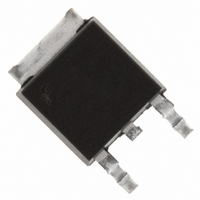
MOSFET P-CH 35V 13A DPAK

FDD6637

Manufacturer Part Number
FDD6637
Description
MOSFET P-CH 35V 13A DPAK
Manufacturer
Fairchild Semiconductor
Series
PowerTrench®r
Datasheet

Specifications of FDD6637

Fet Type
MOSFET P-Channel, Metal Oxide
Fet Feature
Logic Level Gate
Rds On (max) @ Id, Vgs
11.6 mOhm @ 14A, 10V
Drain To Source Voltage (vdss)
35V
Current - Continuous Drain (id) @ 25° C
13A
Vgs(th) (max) @ Id
3V @ 250µA
Gate Charge (qg) @ Vgs
63nC @ 10V
Input Capacitance (ciss) @ Vds
2370pF @ 20V
Power - Max
1.3W
Mounting Type
Surface Mount
Package / Case
DPak, TO-252 (2 leads+tab), SC-63
Configuration
Single
Transistor Polarity
P-Channel
Resistance Drain-source Rds (on)
0.0116 Ohm @ 10 V
Drain-source Breakdown Voltage
35 V
Gate-source Breakdown Voltage
+/- 25 V
Continuous Drain Current
13 A
Power Dissipation
3100 mW
Maximum Operating Temperature
+ 150 C
Mounting Style
SMD/SMT
Minimum Operating Temperature
- 55 C
Lead Free Status / RoHS Status
Lead free / RoHS Compliant
Other names
FDD6637TR

Available stocks

Company
Part Number
Manufacturer
Quantity
Price
Part Number:
FDD6637
Manufacturer:
Fairchild Semiconductor
Quantity:
52 838
Part Number:
FDD6637
Manufacturer:
FAIRCHILD
Quantity:
1 819
Part Number:
FDD6637
Manufacturer:
FAIRCHILD
Quantity:
8 000
Part Number:
FDD6637
Manufacturer:
FAIRCHILD/仙童
Quantity:
20 000
Part Number:
FDD6637
0
Company:
Part Number:
FDD6637
Quantity:
4 500
FDD6637
35V P-Channel PowerTrench MOSFET
General Description
This P-Channel MOSFET has been produced using
Fairchild Semiconductor’s proprietary PowerTrench
technology to deliver low Rdson and optimized Bvdss
capability to offer superior performance benefit in the
applications.
Applications
FDD6637 Rev C2(W)
Absolute Maximum Ratings
Symbol
V
V
V
I
P
T
Thermal Characteristics
R
R
R
Package Marking and Ordering Information
D
2006 Fairchild Semiconductor Corporation
J
DSS
DS(Avalanche)
GSS
D
, T
JC
JA
JA
Device Marking
Inverter
Power Supplies
STG
FDD6637
Drain-Source Voltage
Gate-Source Voltage
Continuous Drain Current
Power Dissipation
Operating and Storage Junction Temperature Range
Thermal Resistance, Junction-to-Case
Thermal Resistance, Junction-to-Ambient
Drain-Source Avalanche Voltage (maximum)
G
S
(TO-252)
D-PAK
TO-252
FDD6637
Device
Parameter
D
@T
@T
Pulsed
@T
@T
@T
C
A
C
A
A
=25°C
=25°C
=25°C
=25°C
=25°C
T
A
=25
D-PAK (TO-252)
o
C unless otherwise noted
Package
(Note 1a)
(Note 1a)
(Note 1b)
(Note 1a)
(Note 1b)
(Note 3)
(Note 3)
(Note 1a)
(Note 1)
(Note 4)
Features
–55 A, –35 V
High performance trench technology for extremely
low R
RoHS Compliant
DS(ON)
Reel Size
13’’
R
R
G
–55 to +150
DS(ON)
DS(ON)
Ratings
–100
–35
–40
–55
–13
3.1
1.3
2.2
Tape width
57
40
96
25
= 11.6 m
= 18 m
12mm
S
D
@ V
@ V
www.fairchildsemi.com
August 2006
GS
GS
= –4.5 V
2500 units
Quantity
= –10 V
Units
C/W
W
V
V
A
V
C

Related parts for FDD6637

FDD6637 Summary of contents

Page 1

... Thermal Resistance, Junction-to-Ambient R JA Thermal Resistance, Junction-to-Ambient R JA Package Marking and Ordering Information Device Marking Device FDD6637 FDD6637 2006 Fairchild Semiconductor Corporation FDD6637 Rev C2(W) Features –55 A, –35 V High performance trench technology for extremely low R DS(ON) RoHS Compliant =25 C unless otherwise noted ...

Page 2

... Turn–On Rise Time r t Turn–Off Delay Time d(off) t Turn–Off Fall Time f Q Total Gate Charge –10V Total Gate Charge – Gate–Source Charge gs Q Gate–Drain Charge gd FDD6637 Rev. C2( 25°C unless otherwise noted A Test Conditions -11 A, L=1mH –250 – ...

Page 3

... Pulse Test: Pulse Width < 300 s, Duty Cycle < 2. Maximum current is calculated as: R DS(ON) where P is maximum power dissipation BV(avalanche) Single-Pulse rating is guaranteed if device is operated within the UIS SOA boundary of the device. FDD6637 Rev. C2( 25°C unless otherwise noted A Test Conditions – – ...

Page 4

... T , JUNCTION TEMPERATURE ( J Figure 3. On-Resistance Variation with Temperature 100 GATE TO SOURCE VOLTAGE (V) GS Figure 5. Transfer Characteristics FDD6637 Rev. C2(W) 2 -3.5V GS 2.2 2 -4.0V 1.8 1.6 -3.5V 1.4 1.2 -3. Figure 2. On-Resistance Variation with Drain Current and Gate Voltage 0.05 0.04 0.03 0.02 ...

Page 5

... 0. DRAIN-SOURCE VOLTAGE (V) DS Figure 9. Maximum Safe Operating Area 100 0.01 0 TIME (sec) 1 Figure 11. Single Pulse Maximum Peak Current FDD6637 Rev. C2(W) 3200 = 10V 30V 2400 20V 1600 800 C rss Figure 8. Capacitance Characteristics 100 100µs 80 1ms 10ms 100ms 0.01 10 100 Figure 10. Single Pulse Maximum ...

Page 6

... SINGLE PULSE 0.001 0.001 0.01 Figure 13. Transient Thermal Response Curve Thermal characterization performed using the conditions described in Note 1b. Transient thermal response will change depending on the circuit board design. FDD6637 Rev. C2(W) 0 TIME (sec ( °C/W ...

Page 7

... Circuit Drain Current Regulator Same type as DUT - 50k 10V DUT I g(REF) Figure 16. Gate Charge Test Circuit GEN V GS Pulse Width 1 s Duty Cycle 0.1 Figure 18. Switching Time Test Circuit FDD6637 Rev. C2( Figure 15. Unclamped Inductive Waveforms 10V 10V - Figure 17. Gate Charge Waveform ...

Page 8

... TRADEMARKS The following are registered and unregistered trademarks Fairchild Semiconductor owns or is authorized to use and is not intended exhaustive list of all such trademarks. ACEx™ FACT Quiet Series™ ActiveArray™ GlobalOptoisolator™ Bottomless™ GTO™ Build it Now™ HiSeC™ ...

Related keywords