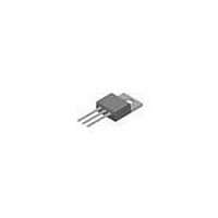
IRF630B_FP001 Fairchild Semiconductor, IRF630B_FP001 Datasheet

IRF630B_FP001
Specifications of IRF630B_FP001
Related parts for IRF630B_FP001
IRF630B_FP001 Summary of contents
Page 1
... Thermal Resistance, Junction-to-Case Max Thermal Resistance, Case-to-Sink Typ Thermal Resistance, Junction-to-Ambient Max. JA ©2002 Fairchild Semiconductor Corporation Features • 9.0A, 200V, R • Low gate charge ( typical 22 nC) • Low Crss ( typical 22 pF) • Fast switching • 100% avalanche tested • Improved dv/dt capability ...
Page 2
... Repetitive Rating : Pulse width limited by maximum junction temperature 3mH 9.0A 50V ≤ 9.0A, di/dt ≤ 300A ≤ DSS, 4. Pulse Test : Pulse width ≤ 300 s, Duty cycle ≤ Essentially independent of operating temperature ©2002 Fairchild Semiconductor Corporation T = 25°C unless otherwise noted C Test Conditions 250 250 A, Referenced to 25° 200 ...
Page 3
... I , Drain Current [A] D Figure 3. On-Resistance Variation vs Drain Current and Gate Voltage 1500 1000 C iss C oss 500 C rss Drain-Source Voltage [V] DS Figure 5. Capacitance Characteristics ©2002 Fairchild Semiconductor Corporation ※ Notes : 1. 250μ s Pulse Test 25℃ Figure 2. Transfer Characteristics 10V GS = 20V ※ Note : ℃ ...
Page 4
... V , Drain-Source Voltage [V] DS Figure 9-1. Maximum Safe Operating Area for IRF630B Case Temperature [ ℃ Figure 10. Maximum Drain Current vs Case Temperature ©2002 Fairchild Semiconductor Corporation (Continued) 3.0 2.5 2.0 1.5 1.0 ※ Notes : 250 μ 0.5 D 0.0 -100 100 150 200 o C] Figure 8 ...
Page 5
... Typical Characteristics Figure 11-1. Transient Thermal Response Curve for IRF630B Figure 11-2. Transient Thermal Response Curve for IRFS630B ©2002 Fairchild Semiconductor Corporation (Continued) ※ θ tio ※ tio ( ℃ (t) θ ( ℃ θ ( θ Rev. B, December 2002 ...
Page 6
... Resistive Switching Test Circuit & Waveforms 10V 10V Unclamped Inductive Switching Test Circuit & Waveforms 10V 10V ©2002 Fairchild Semiconductor Corporation Gate Charge Test Circuit & Waveform Same Type Same Type as DUT as DUT 10V 10V DUT DUT 10% 10 DUT DUT ...
Page 7
... Peak Diode Recovery dv/dt Test Circuit & Waveforms Driver ) ( Driver ) DUT ) ( DUT ) DUT ) ( DUT ) ©2002 Fairchild Semiconductor Corporation + + DUT DUT Driver Driver Same Type Same Type as DUT as DUT • dv/dt controlled by R • dv/dt controlled by R • I • I controlled by pulse period ...
Page 8
... Package Dimensions 9.90 (8.70) ø3.60 1.27 0.10 2.54TYP [2.54 ] 0.20 10.00 ©2002 Fairchild Semiconductor Corporation TO-220 0.20 0.10 1.52 0.10 0.80 0.10 2.54TYP [2.54 ] 0.20 0.20 4.50 0.20 +0.10 1.30 –0.05 +0.10 0.50 2.40 0.20 –0.05 Dimensions in Millimeters Rev. B, December 2002 ...
Page 9
... Package Dimensions (Continued) 10.16 (7.00) MAX1.47 0.80 0.10 #1 0.35 0.10 2.54TYP [2.54 ] 0.20 9.40 ©2002 Fairchild Semiconductor Corporation TO-220F ø3.18 0.20 0.10 (1.00x45 ) 0.50 2.54TYP [2.54 ] 0.20 0.20 2.54 0.20 (0.70) +0.10 2.76 –0.05 0.20 Dimensions in Millimeters Rev. B, December 2002 ...
Page 10
... TRADEMARKS The following are registered and unregistered trademarks Fairchild Semiconductor owns or is authorized to use and is not intended exhaustive list of all such trademarks. ACEx™ FACT™ ActiveArray™ FACT Quiet series™ ® Bottomless™ FAST CoolFET™ FASTr™ CROSSVOLT™ ...


