FDFS2P103 Fairchild Semiconductor, FDFS2P103 Datasheet
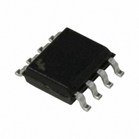
MOSFET P-CH 30V 5.3A 8-SOIC

FDFS2P103

Manufacturer Part Number
FDFS2P103
Description
MOSFET P-CH 30V 5.3A 8-SOIC
Manufacturer
Fairchild Semiconductor
Series
PowerTrench®r
Datasheet

Specifications of FDFS2P103

Fet Type
MOSFET P-Channel, Metal Oxide
Fet Feature
Diode (Isolated)
Rds On (max) @ Id, Vgs
59 mOhm @ 5.3A, 10V
Drain To Source Voltage (vdss)
30V
Current - Continuous Drain (id) @ 25° C
5.3A
Vgs(th) (max) @ Id
3V @ 250µA
Gate Charge (qg) @ Vgs
8nC @ 5V
Input Capacitance (ciss) @ Vds
528pF @ 15V
Power - Max
900mW
Mounting Type
Surface Mount
Package / Case
8-SOIC (3.9mm Width)
Configuration
Single Dual Drain
Transistor Polarity
P-Channel
Resistance Drain-source Rds (on)
0.059 Ohms
Forward Transconductance Gfs (max / Min)
10 S
Drain-source Breakdown Voltage
- 30 V
Gate-source Breakdown Voltage
+/- 25 V
Continuous Drain Current
- 5.3 A
Power Dissipation
2 W
Maximum Operating Temperature
+ 150 C
Mounting Style
SMD/SMT
Minimum Operating Temperature
- 55 C
Lead Free Status / RoHS Status
Lead free / RoHS Compliant
Other names
FDFS2P103TR
FDFS2P103_NL
FDFS2P103_NLTR
FDFS2P103_NLTR

Available stocks

Company
Part Number
Manufacturer
Quantity
Price
Part Number:
FDFS2P103
Manufacturer:
Fairchild Semiconductor
Quantity:
135
FDFS2P103
Integrated P-Channel PowerTrench MOSFET and Schottky Diode
General Description
The
performance of Fairchild's PowerTrench MOSFET
technology with a very low forward voltage drop
Schottky barrier rectifier in an SO-8 package.
This device is designed specifically as a single package
solution for DC to DC converters. It features a fast
switching, low gate charge MOSFET with very low on-
state resistance.
Schottky diode allows its use in a variety of DC/DC
converter topologies.
2001 Fairchild Semiconductor Corporation
Absolute Maximum Ratings
Symbol
V
V
I
P
T
V
I
Package Marking and Ordering Information
D
O
J
DSS
GSS
D
RRM
, T
Device Marking
STG
FDFS2P103
FDFS2P103
SO-8
MOSFET Drain-Source Voltage
MOSFET Gate-Source Voltage
Drain Current
Power Dissipation for Dual Operation
Power Dissipation for Single Operation
Operating and Storage Junction Temperature Range
Schottky Repetitive Peak Reverse Voltage
Schottky Average Forward Current
C
C
The independently connected
combines
Pin 1
D
D
– Continuous
– Pulsed
FDFS2P103
Device
Parameter
A
the
A
S
exceptional
G
T
A
=25
o
C unless otherwise noted
Reel Size
13’’
(Note 1a)
(Note 1a)
(Note 1b)
(Note 1c)
(Note 1a)
Features
–5.3 A, –30V R
V
V
Schottky and MOSFET incorporated into single
Electrically independent Schottky and MOSFET
power surface mount SO-8 package
pinout for design flexibility
F
F
< 0.52 V @ 1 A (T
< 0.57 V @ 1 A (T
G
A
A
S
1
2
4
3
Tape width
R
DS(ON)
DS(ON)
12mm
Ratings
55 to +150
1.6
0.9
J
J
30
5.3
2
1
1
30
25
20
= 125 C)
= 25 C)
= 59 m
= 92 m
September 2001
@ V
@ V
8
7
5
6
GS
GS
C
C
D
D
FDFS2P103 Rev C(W)
= –10 V
= –4.5 V
2500 units
Quantity
Units
W
V
V
A
V
A
C

Related parts for FDFS2P103

FDFS2P103 Summary of contents

Page 1

... =25 C unless otherwise noted A (Note 1a) (Note 1a) (Note 1b) (Note 1c) (Note 1a) Reel Size 13’’ September 2001 = –10 V DS(ON –4.5 V DS(ON 125 Ratings Units – – A 5.3 – 1.6 1 0.9 – +150 Tape width Quantity 12mm 2500 units FDFS2P103 Rev C(W) ...

Page 2

... 1.0 MHz V = – – – GEN V = – –5 – –1.3 A (Note 125 125 C J Typ Max Units V –23 mV/ C –1 A 100 nA –100 nA –1.7 –3 V 4.5 mV 528 pF 132 5 2.2 nC 1.6 nC –1.3 A –0.7 –1 100 0.41 0.57 V 0.32 0.52 V FDFS2P103 Rev C(W) ...

Page 3

... Scale letter size paper 2. Pulse Test: Pulse Width < 300 s, Duty Cycle < 2.0% (Note 1a) (Note 1c) (Note 1) is determined by the user's board design 125°C/W when mounted 0.02 in pad copper 78 C/W 135 C/W 40 C/W c) 135°C/W when mounted on a minimum pad. FDFS2P103 Rev C(W) ...

Page 4

... Figure 6. Body Diode Forward Voltage Variation with Source Current and Temperature. =-4.0V GS -4.5V -5.0V -6.0V -7.0V -8.0V -10V DRAIN CURRENT ( -2. 125 GATE TO SOURCE VOLTAGE (V) GS Gate-to-Source Voltage 125 -55 C 0.2 0.4 0.6 0 BODY DIODE FORWARD VOLTAGE (V) SD FDFS2P103 Rev C( 1.4 ...

Page 5

... Figure 8. Capacitance Characteristics. 1.00E-01 1.00E-02 1.00E-03 1.00E- 1.00E-05 1.00E-06 1.00E-07 0.4 0.5 0.6 0 Figure 10. Schottky Diode Reverse Current. 0 TIM E (sec MHz ISS C OSS DRAIN TO SOURCE VOLTAGE ( 125 REVERSE VOLTAGE ( ( 135 °C/W JA P(pk ( Duty Cycle 100 1000 FDFS2P103 Rev C(W) 60 ...

Page 6

... Intermediate container for 13” reel option Barcode Label sample LOT: CBVK741B019 FSID: FDS9953A D/C1: Z9842AB QTY1: SPEC REV: D/C2: QTY2: CPN: FAIRCHILD SEMICONDUCTOR CORPORATION Components F 852 NDS 9959 Pin 1 Barcode Label Barcode Label QTY: 2500 SPEC: (F63T NR) ...

Page 7

SOIC(8lds) Embossed Carrier Tape Configuration: Figure 3 Pkg type SOIC(8lds) 5.30 6.50 12.0 +/-0.10 +/-0.10 +/-0.3 (12mm) Notes: A0, B0, and K0 dimensions are determined with respect to the EIA/Jedec RS-481 rotational ...

Page 8

... SOIC-8 Package Dimensions SOIC-8 (FS PKG Code S1) 9 ©2000 Fairchild Semiconductor International Scale 1:1 on letter size paper Dimensions shown below are in: inches [millimeters] Part Weight per unit (gram): 0.0774 September 1998, Rev. A ...

Page 9

... TRADEMARKS The following are registered and unregistered trademarks Fairchild Semiconductor owns or is authorized to use and is not intended exhaustive list of all such trademarks. ACEx™ FAST Bottomless™ FASTr™ FRFET™ CoolFET™ GlobalOptoisolator™ CROSSVOLT™ GTO™ DenseTrench™ ...

Related keywords