FQPF6N80 Fairchild Semiconductor, FQPF6N80 Datasheet - Page 2
FQPF6N80
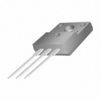
Manufacturer Part Number
FQPF6N80
Description
MOSFET N-CH 800V 3.3A TO-220F
Manufacturer
Fairchild Semiconductor
Series
QFET™r
Datasheet
1.FQPF6N80T.pdf
(8 pages)
Specifications of FQPF6N80
Fet Type
MOSFET N-Channel, Metal Oxide
Fet Feature
Standard
Rds On (max) @ Id, Vgs
1.95 Ohm @ 1.65A, 10V
Drain To Source Voltage (vdss)
800V
Current - Continuous Drain (id) @ 25° C
3.3A
Vgs(th) (max) @ Id
5V @ 250µA
Gate Charge (qg) @ Vgs
31nC @ 10V
Input Capacitance (ciss) @ Vds
1500pF @ 25V
Power - Max
51W
Mounting Type
Through Hole
Package / Case
TO-220-3 Full Pack (Straight Leads)
Lead Free Status / RoHS Status
Lead free / RoHS Compliant
Available stocks
Company
Part Number
Manufacturer
Quantity
Price
Company:

Part Number:
FQPF6N80
Manufacturer:
FAIRCHILD
Quantity:
12 500
Company:
Part Number:
FQPF6N80C
Manufacturer:
IR
Quantity:
5 000
Company:
Part Number:
FQPF6N80C
Manufacturer:
Fairchi/ON
Quantity:
17 423
Part Number:
FQPF6N80C
Manufacturer:
ON/安森美
Quantity:
20 000
Company:
Part Number:
FQPF6N80T
Manufacturer:
Fairchi/ON
Quantity:
17 456


©2000 Fairchild Semiconductor International
Electrical Characteristics
Notes:
1. Repetitive Rating : Pulse width limited by maximum junction temperature
2. L = 117mH, I
3. I
4. Pulse Test : Pulse width ≤ 300 s, Duty cycle ≤ 2%
5. Essentially independent of operating temperature
Off Characteristics
BV
/
I
I
I
On Characteristics
V
R
g
Dynamic Characteristics
C
C
C
Switching Characteristics
t
t
t
t
Q
Q
Q
Drain-Source Diode Characteristics and Maximum Ratings
I
I
V
t
Q
Symbol
DSS
GSSF
GSSR
d(on)
r
d(off)
f
S
SM
rr
SD
FS
BV
GS(th)
SD
DS(on)
iss
oss
rss
g
gs
gd
rr
DSS
≤ 5.8A, di/dt ≤ 200A/ s, V
DSS
T
J
AS
Drain-Source Breakdown Voltage
Breakdown Voltage Temperature
Coefficient
Zero Gate Voltage Drain Current
Gate-Body Leakage Current, Forward
Gate-Body Leakage Current, Reverse
Gate Threshold Voltage
Static Drain-Source
On-Resistance
Forward Transconductance
Input Capacitance
Output Capacitance
Reverse Transfer Capacitance
Turn-On Delay Time
Turn-On Rise Time
Turn-Off Delay Time
Turn-Off Fall Time
Total Gate Charge
Gate-Source Charge
Gate-Drain Charge
Maximum Continuous Drain-Source Diode Forward Current
Maximum Pulsed Drain-Source Diode Forward Current
Drain-Source Diode Forward Voltage
Reverse Recovery Time
Reverse Recovery Charge
= 3.3A, V
DD
= 50V, R
DD
Parameter
≤ BV
G
= 25
DSS,
Starting T
Starting T
J
T
= 25°C
J
C
= 25°C
= 25°C unless otherwise noted
V
I
V
V
V
V
V
V
V
V
f = 1.0 MHz
V
R
V
V
V
V
dI
D
GS
DS
DS
GS
GS
DS
GS
DS
DS
DD
DS
GS
GS
GS
G
F
= 250 A, Referenced to 25°C
/ dt = 100 A/ s
= 25
= 10 V, I
= 800 V, V
= 640 V, T
= V
= 50 V, I
= 25 V, V
= 640 V, I
= 0 V, I
= 30 V, V
= -30 V, V
= 400 V, I
= 10 V
= 0 V, I
= 0 V, I
Test Conditions
GS
, I
D
D
S
S
D
D
= 1.65 A
= 250 A
= 3.3 A
= 5.8 A,
GS
DS
D
D
= 250 A
DS
= 1.65 A
GS
C
= 5.8 A,
= 5.8 A,
= 125°C
= 0 V
= 0 V,
= 0 V
= 0 V
(Note 4, 5)
(Note 4, 5)
(Note 4)
(Note 4)
Min
800
3.0
--
--
--
--
--
--
--
--
--
--
--
--
--
--
--
--
--
--
--
--
--
--
1150
Typ
125
650
0.9
1.5
4.3
7.1
5.7
14
30
70
65
45
31
15
--
--
--
--
--
--
--
--
--
1500
-100
Max
1.95
13.2
100
100
160
150
140
100
5.0
3.3
1.4
10
18
70
--
--
--
--
--
--
--
Rev. A, September 2000
Units
V/°C
nA
nA
nC
nC
nC
pF
pF
pF
ns
ns
ns
ns
ns
V
V
S
A
A
V
C
A
A
Related parts for FQPF6N80
Image
Part Number
Description
Manufacturer
Datasheet
Request
R

Part Number:
Description:
Fairchild Semiconductor [IGBT MODULE]
Manufacturer:
Fairchild Semiconductor
Datasheet:

Part Number:
Description:
Discrete Semiconductor Modules
Manufacturer:
Fairchild Semiconductor
Part Number:
Description:
Discrete Semiconductor Modules
Manufacturer:
Fairchild Semiconductor
Part Number:
Description:
This N-Channel MOSFET is produced using Fairchild Semiconductor’s advanced Power Trench® process
Manufacturer:
Fairchild Semiconductor
Datasheet:
Part Number:
Description:
This N-Channel MOSFET is produced using Fairchild Semiconductor’s advanced Power Trench® process
Manufacturer:
Fairchild Semiconductor
Datasheet:
Part Number:
Description:
This N-Channel MOSFET is produced using Fairchild Semiconductor’s advanced PowerTrench® process
Manufacturer:
Fairchild Semiconductor
Datasheet:
Part Number:
Description:
This N-Channel MOSFET is produced using Fairchild Semiconductor’s advanced PowerTrench® process
Manufacturer:
Fairchild Semiconductor
Datasheet:
Part Number:
Description:
This N-Channel MOSFET is produced using Fairchild Semiconductor’s advanced Power Trench® process
Manufacturer:
Fairchild Semiconductor
Datasheet:
Part Number:
Description:
This N-Channel logic Level MOSFETs are produced using Fairchild Semiconductor‘s advanced Power Trench® process that has been special tailored to minimize the on-state resistance and yet maintain superior switching performance
Manufacturer:
Fairchild Semiconductor
Datasheet:
Part Number:
Description:
This N-Channel MOSFET is produced using Fairchild Semiconductor’s advanced Power Trench® process
Manufacturer:
Fairchild Semiconductor
Datasheet:
Part Number:
Description:
This N-Channel SyncFET™ is produced using Fairchild Semiconductor’s advanced PowerTrench® process
Manufacturer:
Fairchild Semiconductor
Datasheet:
Part Number:
Description:
This N-Channel SyncFET™ is produced using Fairchild Semiconductor’s advanced PowerTrench® process
Manufacturer:
Fairchild Semiconductor
Datasheet:
Part Number:
Description:
This N-Channel SyncFET™ is produced using Fairchild Semiconductor’s advanced PowerTrench® process
Manufacturer:
Fairchild Semiconductor
Datasheet:
Part Number:
Description:
This N-Channel logic Level MOSFETs are produced using Fairchild Semiconductor‘s advanced Power Trench® process that has been special tailored to minimize the on-state resistance and yet maintain superior switching performance
Manufacturer:
Fairchild Semiconductor
Datasheet:
Part Number:
Description:
This N-Channel MOSFET is produced using Fairchild Semiconductor’s advanced Power Trench® process that has been especially tailored to minimize the on-state resistance and yet maintain superior switching performance
Manufacturer:
Fairchild Semiconductor
Datasheet: