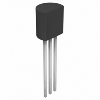
IRFN214BTA_FP001 Fairchild Semiconductor, IRFN214BTA_FP001 Datasheet - Page 3

IRFN214BTA_FP001
Manufacturer Part Number
IRFN214BTA_FP001
Description
MOSFET N-CH 250V 0.6A TO-92
Manufacturer
Fairchild Semiconductor
Datasheet
1.IRFN214BTA_FP001.pdf
(8 pages)
Specifications of IRFN214BTA_FP001
Fet Type
MOSFET N-Channel, Metal Oxide
Fet Feature
Standard
Rds On (max) @ Id, Vgs
2 Ohm @ 300mA, 10V
Drain To Source Voltage (vdss)
250V
Current - Continuous Drain (id) @ 25° C
600mA
Vgs(th) (max) @ Id
4V @ 250µA
Gate Charge (qg) @ Vgs
10.5nC @ 10V
Input Capacitance (ciss) @ Vds
275pF @ 25V
Power - Max
1.8W
Mounting Type
Through Hole
Package / Case
TO-92-3 (Standard Body), TO-226
Lead Free Status / RoHS Status
Lead free / RoHS Compliant
©2004 Fairchild Semiconductor Corporation
Typical Characteristics
10
10
10
500
400
300
200
100
-1
-2
0
10
10
0
8
6
4
2
0
10
-1
Top :
Bottom :
0
Figure 5. Capacitance Characteristics
-1
Figure 3. On-Resistance Variation vs
Figure 1. On-Region Characteristics
Drain Current and Gate Voltage
15.0 V
10.0 V
8.0 V
6.0 V
5.0 V
4.5 V
4.0 V
V
GS
2
V
V
DS
DS
, Drain-Source Voltage [V]
, Drain-Source Voltage [V]
10
I
10
D
0
, Drain Current [A]
0
C
C
C
iss
rss
oss
V
4
GS
V
= 20V
GS
= 10V
C
C
C
※
iss
oss
rss
1. 250µs Pulse Test
2. T
10
10
= C
Notes :
= C
= C
※
6
1
1
A
gs
gd
ds
= 25 ℃
Note : T
+ C
+ C
※
gd
1. V
2. f = 1 MHz
gd
Notes :
(C
J
GS
= 25 ℃
ds
= shorted)
= 0 V
8
10
10
10
10
12
10
8
6
4
2
0
-1
-1
0
0
0.0
0.2
2
Figure 4. Body Diode Forward Voltage
Figure 6. Gate Charge Characteristics
Figure 2. Transfer Characteristics
150
25
o
C
0.4
Variation with Source Current
o
C
1.5
150 ℃
4
0.6
V
V
and Temperature
Q
GS
SD
3.0
G
, Source-Drain voltage [V]
, Gate-Source Voltage [V]
, Total Gate Charge [nC]
-55
V
25 ℃
DS
V
o
0.8
C
DS
= 200V
V
= 125V
DS
4.5
6
= 50V
1.0
6.0
※
1.2
※
1. V
2. 250µs Pulse Test
1. V
2. 250µs Pulse Test
Notes :
Notes :
8
※
DS
G S
Note : I
= 40V
= 0V
7.5
1.4
D
= 0.5 A
1.6
10
Rev. A, May 2004
9.0


