PSMN004-55W,127 NXP Semiconductors, PSMN004-55W,127 Datasheet - Page 2
PSMN004-55W,127
Manufacturer Part Number
PSMN004-55W,127
Description
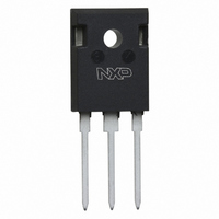
MOSFET N-CH 55V 100A SOT429
Manufacturer
NXP Semiconductors
Series
TrenchMOS™r
Datasheet
1.PSMN004-55W127.pdf
(8 pages)
Specifications of PSMN004-55W,127
Fet Type
MOSFET N-Channel, Metal Oxide
Fet Feature
Logic Level Gate
Rds On (max) @ Id, Vgs
4.2 mOhm @ 25A, 10V
Drain To Source Voltage (vdss)
55V
Current - Continuous Drain (id) @ 25° C
100A
Vgs(th) (max) @ Id
2V @ 1mA
Gate Charge (qg) @ Vgs
226nC @ 5V
Input Capacitance (ciss) @ Vds
13000pF @ 25V
Power - Max
300W
Mounting Type
Through Hole
Package / Case
TO-247-3
Lead Free Status / RoHS Status
Lead free / RoHS Compliant
Other names
934055815127
PSMN004-55W
PSMN004-55W
PSMN004-55W
PSMN004-55W


Philips Semiconductors
AVALANCHE ENERGY LIMITING VALUES
Limiting values in accordance with the Absolute Maximum System (IEC 134)
THERMAL RESISTANCES
ELECTRICAL CHARACTERISTICS
T
October 1999
N-channel logic level TrenchMOS
SYMBOL PARAMETER
E
I
SYMBOL PARAMETER
R
R
SYMBOL PARAMETER
V
V
R
I
I
Q
Q
Q
t
t
t
t
L
L
L
C
C
C
j
AS
= 25˚C unless otherwise specified
GSS
DSS
d on
r
d off
f
d
d
s
AS
(BR)DSS
GS(TO)
th j-mb
th j-a
DS(ON)
iss
oss
rss
g(tot)
gs
gd
Non-repetitive avalanche
energy
Non-repetitive avalanche
current
Thermal resistance junction
to mounting base
Thermal resistance junction
to ambient
Drain-source breakdown
voltage
Gate threshold voltage
Drain-source on-state
resistance
Gate-source leakage current V
Zero gate voltage drain
current
Total gate charge
Gate-source charge
Gate-drain (Miller) charge
Turn-on delay time
Turn-on rise time
Turn-off delay time
Turn-off fall time
Internal drain inductance
Internal drain inductance
Internal source inductance
Input capacitance
Output capacitance
Feedback capacitance
CONDITIONS
Unclamped inductive load, I
t
V
fig:15
CONDITIONS
in free air
CONDITIONS
V
V
V
V
V
V
V
I
V
V
Resistive load
Measured tab to centre of die
Measured from drain lead to centre of die
Measured from source lead to source
bond pad
V
p
D
DD
GS
DS
GS
GS
GS
GS
GS
DS
DD
GS
GS
= 100 A; V
= 100 s; T
= 0 V; I
= V
= 10 V; I
= 5 V; I
= 4.5 V; I
= 5 V; I
= 10 V; V
= 55 V; V
= 30 V; R
= 10 V; R
= 0 V; V
25 V; R
GS
transistor
; I
D
D
D
D
DS
D
DD
= 0.25 mA;
= 1 mA
= 25 A
= 25 A; T
D
j
GS
GS
D
G
= 25 A
prior to avalanche = 25˚C;
2
DS
= 25 V; f = 1 MHz
= 25 A
= 44 V; V
= 1.2 ;
= 5.6
= 0 V;
= 50 ; V
= 0 V;
j
= 175˚C
GS
GS
= 5 V
AS
= 5 V; refer to
= 100 A;
T
T
T
T
j
j
j
j
= 175˚C
= 175˚C
= -55˚C
= -55˚C
MIN.
MIN.
0.5
55
42
MIN.
1
-
-
-
-
-
-
-
-
-
-
-
-
-
-
-
-
-
-
-
-
-
-
-
-
-
PSMN004-55W
TYP. MAX. UNIT
TYP. MAX. UNIT
1900
1250
0.02
0.05
Product specification
226
106
118
848
336
1.5
3.2
3.6
3.8
6.2
3.5
4.5
7.5
45
36
26
13
-
-
-
-
-
-
MAX.
357
100
100
500
0.5
2.3
4.2
4.5
9.5
10
2
5
-
-
-
-
-
-
-
-
-
-
-
-
-
-
-
-
-
Rev 1.100
UNIT
mJ
K/W
K/W
A
m
m
m
m
nA
nC
nC
nC
nH
nH
nH
nF
pF
pF
ns
ns
ns
ns
V
V
V
V
V
A
A
Related parts for PSMN004-55W,127
Image
Part Number
Description
Manufacturer
Datasheet
Request
R

Part Number:
Description:
SiliconMAX standard level N-channel enhancement mode Field-Effect Transistor (FET) in a plastic package using TrenchMOS technology
Manufacturer:
NXP Semiconductors
Datasheet:

Part Number:
Description:
N-channel TrenchMOS SiliconMAX logic level FET
Manufacturer:
NXP [NXP Semiconductors]
Datasheet:

Part Number:
Description:
Psmn004-55w N-channel Logic Level Trenchmos Tm Transistor
Manufacturer:
NXP Semiconductors
Datasheet:

Part Number:
Description:
MOSFET N-CH 60V 75A TO220AB
Manufacturer:
NXP Semiconductors
Datasheet:

Part Number:
Description:
MOSFET N-CH 60V 75A D2PAK
Manufacturer:
NXP Semiconductors
Datasheet:
Part Number:
Description:
MOSFET N-CH 36V 75A SOT404
Manufacturer:
NXP Semiconductors
Datasheet:
Part Number:
Description:
MOSFET TAPE13 PWR-MOS
Manufacturer:
NXP Semiconductors
Datasheet:
Part Number:
Description:
N-channel enhancement mode field-effect transistor
Manufacturer:
NXP Semiconductors
Datasheet:
Part Number:
Description:
N-channel Enhancement Mode Field-effect Transistor
Manufacturer:
NXP Semiconductors
Datasheet:
Part Number:
Description:
NXP Semiconductors designed the LPC2420/2460 microcontroller around a 16-bit/32-bitARM7TDMI-S CPU core with real-time debug interfaces that include both JTAG andembedded trace
Manufacturer:
NXP Semiconductors
Datasheet:

Part Number:
Description:
NXP Semiconductors designed the LPC2458 microcontroller around a 16-bit/32-bitARM7TDMI-S CPU core with real-time debug interfaces that include both JTAG andembedded trace
Manufacturer:
NXP Semiconductors
Datasheet:
Part Number:
Description:
NXP Semiconductors designed the LPC2468 microcontroller around a 16-bit/32-bitARM7TDMI-S CPU core with real-time debug interfaces that include both JTAG andembedded trace
Manufacturer:
NXP Semiconductors
Datasheet:
Part Number:
Description:
NXP Semiconductors designed the LPC2470 microcontroller, powered by theARM7TDMI-S core, to be a highly integrated microcontroller for a wide range ofapplications that require advanced communications and high quality graphic displays
Manufacturer:
NXP Semiconductors
Datasheet:
Part Number:
Description:
NXP Semiconductors designed the LPC2478 microcontroller, powered by theARM7TDMI-S core, to be a highly integrated microcontroller for a wide range ofapplications that require advanced communications and high quality graphic displays
Manufacturer:
NXP Semiconductors
Datasheet:
Part Number:
Description:
The Philips Semiconductors XA (eXtended Architecture) family of 16-bit single-chip microcontrollers is powerful enough to easily handle the requirements of high performance embedded applications, yet inexpensive enough to compete in the market for hi
Manufacturer:
NXP Semiconductors
Datasheet: