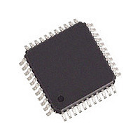
82V2081PPG8 IDT, Integrated Device Technology Inc, 82V2081PPG8 Datasheet - Page 10

82V2081PPG8
Manufacturer Part Number
82V2081PPG8
Description
Manufacturer
IDT, Integrated Device Technology Inc
Datasheet
1.82V2081PPG8.pdf
(68 pages)
Specifications of 82V2081PPG8
Number Of Transceivers
1
Screening Level
Industrial
Mounting
Surface Mount
Package Type
TQFP
Operating Temperature (min)
-40C
Operating Temperature (max)
85C
Lead Free Status / RoHS Status
Compliant
SINGLE CHANNEL T1/E1/J1 LONG HAUL/SHORT HAUL LINE INTERFACE UNIT
Table-1 Pin Description (Continued)
RXTXM1
MODE1
MODE0
RCLKE
MCLK
Name
LOS
REF
CS
Type
O
I
I
I
I
I
Pin No.
43
17
16
21
11
9
7
MCLK: Master Clock input
A built-in clock system that accepts selectable 2.048MHz reference for E1 operating mode and 1.544MHz reference for T1/J1
operating mode. This reference clock is used to generate several internal reference signals:
•
•
•
•
•
•
The loss of MCLK will turn TTIP/TRING into high impedance status.
LOS: Loss of Signal Output
This is an active high signal used to indicate the loss of received signal. When LOS pin becomes high, it indicates the loss of
received signal. The LOS pin will become low automatically when valid received signal is detected again. The criteria of loss
of signal are described in
REF: reference resister
An external resistor (3KΩ, 1%) is used to connect this pin to ground to provide a standard reference current for internal circuit.
MODE[1:0]: operation mode of Control interface select
The level on this pin determines which control mode is used to control the device as follows:
•
•
•
RCLKE: the active edge of RCLK select
In hardware control mode, this pin selects the active edge of RCLK
•
•
In software control mode, this pin should be connected to GNDIO.
CS: Chip Select
In serial or parallel microcontroller interface mode, this is the active low enable signal. A low level on this pin enables serial or
parallel microcontroller interface.
RXTXM[1:0]: Receive and transmit path operation mode select
In hardware control mode, these pins are used to select the single rail or dual rail operation modes as well as AMI or HDB3/
B8ZS line coding:
•
•
•
•
Timing reference for the integrated clock recovery unit.
Timing reference for the integrated digital jitter attenuator.
Timing reference for microcontroller interface.
Generation of RCLK signal during a loss of signal condition.
Reference clock to transmit All Ones, all zeros, PRBS/QRSS pattern as well as activate or deactivate Inband Loopback
code if MCLK is selected as the reference clock. Note that for ATAO and AIS, MCLK is always used as the reference
clock.
Reference clock during the Transmit All Ones (TAO) condition or sending PRBS/QRSS in hardware control mode.
The serial microcontroller Interface consists of CS, SCLK, SCLKE, SDI, SDO and INT pins. SCLKE is used for the
selection of the active edge of SCLK.
The parallel multiplexed microcontroller interface consists of CS, AD[7:0], DS/RD, R/W/WR, ALE/AS, ACK/RDY and
INT pins. (refer to
Hardware interface consists of PULS[3:0], THZ, RCLKE, LP[1:0], PATT[1:0], JA[1:0], MONT, TERM, EQ, RPD,
MODE[1:0] and RXTXM[1:0]
L= select the rising edge as the active edge of RCLK
H= select the falling edge as the active edge of RCLK
00= single rail with HDB3/B8ZS coding
01= single rail with AMI coding
10= dual rail interface with CDR enabled
11= slicer mode (dual rail interface with CDR disabled)
MODE[1:0]
00
01
10
11
3.12 MICROCONTROLLER INTERFACES
3.6 LOS AND AIS
Hardware interface
Serial Microcontroller Interface
Parallel –Multiplexed -Motorola Interface
Parallel –Multiplexed -Intel Interface
10
DETECTION.
Control Interface mode
Description
for details)
TEMPERATURE RANGES
INDUSTRIAL


