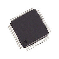
82V2081PPG8 IDT, Integrated Device Technology Inc, 82V2081PPG8 Datasheet - Page 22

82V2081PPG8
Manufacturer Part Number
82V2081PPG8
Description
Manufacturer
IDT, Integrated Device Technology Inc
Datasheet
1.82V2081PPG8.pdf
(68 pages)
Specifications of 82V2081PPG8
Number Of Transceivers
1
Screening Level
Industrial
Mounting
Surface Mount
Package Type
TQFP
Operating Temperature (min)
-40C
Operating Temperature (max)
85C
Lead Free Status / RoHS Status
Compliant
SINGLE CHANNEL T1/E1/J1 LONG HAUL/SHORT HAUL LINE INTERFACE UNIT
impedance matching for both receiver and transmitter. If TERM pin is low,
external impedance network will be used for impedance matching. If TERM
pin is high, internal impedance will be used for impedance matching and
PULS[3:0] pins can be set to select the specific internal impedance. Refer
to
3.4.2
ing on channels located in other chips can be performed by tapping the mon-
itored channel through a high impedance bridging circuit. Refer to
9
RRING is dramatically attenuated. To compensate this attenuation, the
Monitor Gain can be used to boost the signal by 22 dB, 26 dB and 32 dB,
selected by MG[1:0] bits (RCF2, 0CH). For normal operation, the Monitor
Gain should be set to 0 dB.
Gain. When MONT pin is low, the Monitor Gain is 0 dB. When MONT pin
is high, the Monitor Gain is 26 dB. Refer to
SUMMARY
and Figure-11.
5 HARDWARE CONTROL PIN SUMMARY
Figure-9 Monitoring Receive Line in Another Chip
In hardware control mode, TERM, PULS[3:0] pins can be used to select
In both T1/J1 and E1 short haul applications, the non-intrusive monitor-
After a high resistance bridging circuit, the signal arriving at the RTIP/
In hardware control mode, MONT pin can be used to set the Monitor
Figure-10 Monitor Transmit Line in Another Chip
LINE MONITOR
DSX cross connect
DSX cross connect
for details.
point
point
R
R
5 HARDWARE CONTROL PIN
TTIP
RTIP
TRING
RRING
for details.
RRING
RRING
RTIP
RTIP
=22/26/32dB
monitor gain
monitor gain
monitor mode
normal transmit mode
normal receive mode
gain=0dB
=22/26/32dB
monitor gain
monitor
monitor mode
Figure-
22
3.4.3
intersymbol interference caused by cable attenuation. It can be enabled or
disabled by setting EQ_ON bit to ‘1’ or ‘0’ (RCF1, 0BH).
be set to ‘1’ to indicate the status of equalizer. If EQ_IES bit (INTES, 16H)
is set to ‘1’, any changes of EQ_S bit will generate an interrupt and EQ_IS
bit (INTS0, 19H) will be set to ‘1’ if it is not masked. If EQ_IES is set to ‘0’,
only the ‘0’ to ‘1’ transition of the EQ_S bit will generate an interrupt and
EQ_IS bit will be set to ‘1’ if it is not masked. The EQ_IS bit will be reset after
being read.
tude/wave shape of the incoming signals during an observation period. This
observation period can be 32, 64, 128 or 256 symbol periods, as selected
by UPDW[1:0] bits (RCF2, 0CH). A shorter observation period allows
quicker responses to pulse amplitude variation while a longer observation
period can minimize the possible overshoots. The default observation
period is 128 symbol periods.
adjusted to achieve a normalized signal. LATT[4:0] bits (STAT1, 18H) indi-
cate the signal attenuation introduced by the cable in approximately 2 dB
per step.
3.4.4
J1 is -10 dB. For long haul application, the receive sensitivity is -43 dB for
E1 and -36 dB for T1/J1.
operating mode can be selected by setting EQ pin. For short haul mode,
the Receive Sensitivity for both E1 and T1/J1 is -10 dB. For long haul mode,
the receive sensitivity is -43 dB for E1 and -36 dB for T1/J1. Refer to
WARE CONTROL PIN SUMMARY
3.4.5
space according to the amplitude of the input signals. The threshold can
be 40%, 50%, 60% or 70%, as selected by the SLICE[1:0] bits (RCF2, 0CH).
The output of the Data Slicer is forwarded to the CDR (Clock & Data Recov-
ery) unit or to the RDP/RDN pins directly if the CDR is disabled.
3.4.6
The recovered clock tracks the jitter in the data output from the Data Slicer
and keeps the phase relationship between data and clock during the
absence of the incoming pulse. The CDR can also be by-passed in the Dual
Rail mode. When CDR is by-passed, the data from the Data Slicer is output
to the RDP/RDN pins directly.
3.4.7
the AMI decoder or B8ZS decoder. In E1 applications, the R_MD[1:0] bits
(RCF0, 0AH) are used to select the AMI decoder or HDB3 decoder.
and transmit path can be selected by setting RXTXM1 and RXTXM0 pins.
Refer to
The adaptive equalizer can remove most of the signal distortion due to
When the adaptive equalizer is out of range, EQ_S bit (STAT0, 17H) will
The Amplitude/wave shape detector keeps on measuring the ampli-
Based on the observed peak value for a period, the equalizer will be
For short haul application, the Receive Sensitivity for both E1 and T1/
When the chip is configured by hardware, the short haul or long haul
The Data Slicer is used to generate a standard amplitude mark or a
The CDR is used to recover the clock and data from the received signal.
In T1/J1 applications, the R_MD[1:0] bits (RCF0, 0AH) is used to select
When the chip is configured by hardware, the operation mode of receive
ADAPTIVE EQUALIZER
RECEIVE SENSITIVITY
DATA SLICER
CDR (Clock & Data Recovery)
DECODER
5 HARDWARE CONTROL PIN SUMMARY
for details.
TEMPERATURE RANGES
for details.
INDUSTRIAL
5 HARD-


