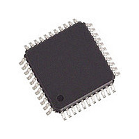
82V2081PPG8 IDT, Integrated Device Technology Inc, 82V2081PPG8 Datasheet - Page 20

82V2081PPG8
Manufacturer Part Number
82V2081PPG8
Description
Manufacturer
IDT, Integrated Device Technology Inc
Datasheet
1.82V2081PPG8.pdf
(68 pages)
Specifications of 82V2081PPG8
Number Of Transceivers
1
Screening Level
Industrial
Mounting
Surface Mount
Package Type
TQFP
Operating Temperature (min)
-40C
Operating Temperature (max)
85C
Lead Free Status / RoHS Status
Compliant
SINGLE CHANNEL T1/E1/J1 LONG HAUL/SHORT HAUL LINE INTERFACE UNIT
Table-13 Transmit Waveform Value For DS1 -22.5 dB LBO
3.3.4
impedance matching can be realized by the internal impedance matching
circuit or the external impedance matching circuit. If T_TERM[2] is set to
Table-14 Impedance Matching for Transmitter
3.3.5
05H) to ‘1’. In this case, the TTIP/TRING pins are turned into high imped-
ance.
SCAL[5:0] = 000100 (default), One step change of this value of SCAL[5:0]
results in 25% scaling up/down against the pulse amplitude.
The transmit line interface consists of TTIP pin and TRING pin. The
Note: The precision of the resistors should be better than ± 1%
The transmit path can be powered down by setting the T_OFF bit (TCF0,
Sample
10
12
13
14
15
16
11
Cable Configuration
1
2
3
4
5
6
7
8
9
TRANSMIT PATH LINE INTERFACE
TRANSMIT PATH POWER DOWN
T1/133~266 ft
T1/266~399 ft
T1/399~533 ft
T1/533~655 ft
-15.0 dB LBO
-22.5 dB LBO
-7.5 dB LBO
T1/0~133 ft
J1/0~655 ft
E1/120 Ω
0 dB LBO
E1/75 Ω
0000000
0000000
0000000
0000000
0000001
0010101
0100000
0101010
0000011
0000111
0001011
0011001
0011100
0100011
0100111
0001111
UI 1
0101100
0110000
0110001
0110010
0110010
0110010
0110001
0110000
0101100
0101001
0100100
0100010
0100000
0101110
0101110
0100111
UI 2
T_TERM[2:0]
000
001
010
010
011
0011010
0011000
0010101
0010100
0010011
0010001
0010000
0001101
0001100
0001010
0001001
0011110
0011100
0010111
0001111
0001110
UI 3
Internal Termination
0001000
0000110
0000101
0000101
0000100
0000100
0000011
0000011
0000010
0000010
0000010
0000001
0000001
0000001
0000001
0000111
PULS[3:0]
UI 4
0000
0001
0010
0100
0101
1000
1001
1010
0011
0110
0111
1011
20
‘0’, the internal impedance matching circuit will be selected. In this case,
the T_TERM[1:0] bits (TERM, 03H) can be set to choose 75 Ω, 100 Ω, 110
Ω or 120 Ω internal impedance of TTIP/TRING. If T_TERM[2] is set to ‘1’,
the internal impedance matching circuit will be disabled. In this case, the
external impedance matching circuit will be used to realize the impedance
matching. For T1/J1 mode, the external impedance matching circuit for the
transmitter is not supported.
ponents to connect with the cable.
impedance matching for transmitter.
matching for both receiver and transmitter. If TERM pin is low, external
impedance network will be used for impedance matching. If TERM pin is
high, internal impedance will be used for impedance matching and
PULS[3:0] pins will be set to select the specific internal impedance. Refer
to
the THZ bit (TCF1, 06H) to ‘1’. In this state, the internal transmit circuits are
still active.
ance by pulling THZ pin to high. Refer to
SUMMARY
high impedance:
•
•
•
•
pulling both PATT1 and PATT0 pins to high. Refer to
TROL PIN SUMMARY
0 Ω
R
5 HARDWARE CONTROL PIN SUMMARY
In hardware control mode, TERM pin can be used to select impedance
The TTIP/TRING pins can also be turned into high impedance by setting
In hardware control mode, TTIP/TRING can be turned into high imped-
Besides, in the following cases, both TTIP/TRING pins will also become
T
In hardware control mode, the transmit path can be powered down by
Loss of MCLK;
Loss of TCLK (exceptions: Remote Loopback; Transmit internal
pattern by MCLK);
Transmit path power down;
After software reset; pin reset and power on.
for details.
T_TERM[2:0]
1XX
-
for details.
Figure-8
External Termination
Table-14
shows the appropriate external com-
PULS[3:0]
0001
0001
5 HARDWARE CONTROL PIN
-
TEMPERATURE RANGES
is the list of the recommended
for details.
5 HARDWARE CON-
INDUSTRIAL
9.4 Ω
R
-
T


