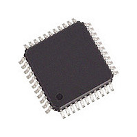
82V2081PPG8 IDT, Integrated Device Technology Inc, 82V2081PPG8 Datasheet - Page 23

82V2081PPG8
Manufacturer Part Number
82V2081PPG8
Description
Manufacturer
IDT, Integrated Device Technology Inc
Datasheet
1.82V2081PPG8.pdf
(68 pages)
Specifications of 82V2081PPG8
Number Of Transceivers
1
Screening Level
Industrial
Mounting
Surface Mount
Package Type
TQFP
Operating Temperature (min)
-40C
Operating Temperature (max)
85C
Lead Free Status / RoHS Status
Compliant
SINGLE CHANNEL T1/E1/J1 LONG HAUL/SHORT HAUL LINE INTERFACE UNIT
3.4.8
and RDN pin. In E1 mode, the RCLK outputs a recovered 2.048 MHz clock.
In T1/J1 mode, the RCLK outputs a recovered 1.544 MHz clock. The
received data is updated on the RD/RDP and RDN pins on the active edge
of RCLK. The active edge of RCLK can be selected by the RCLK_SEL bit
(RCF0, 0AH). And the active level of the data on RD/RDP and RDN can be
selected by the RD_INV bit (RCF0, 0AH).
selected. If RCLKE is set to high, the falling edge will be chosen as the active
edge of RCLK. If RCLKE is set to low, the rising edge will be chosen as the
active edge of RCLK. The active level of the data on RD/RDP and RDN is
the same as that in software control mode.
Single Rail or Dual Rail, as selected by R_MD bit [1] (RCF0, 0AH). In Single
Rail mode, only RD pin is used to output data and the RDN/CV pin is used
to report the received errors. In Dual Rail Mode, both RDP pin and RDN pin
are used for outputting data.
R_MD[1:0] to ‘11’ (binary). In this situation, the output data from the Data
Slicer will be output to the RDP/RDN pins directly, and the RCLK outputs
the exclusive OR (XOR) of the RDP and RDN. This is called receiver slicer
mode. In this case, the transmit path is still operating in Dual Rail mode.
3.4.9
0AH) to ‘1’. In this case, the RCLK, RD/RDP, RDN and LOS will be logic low.
ing RPD pin to high. Refer to
for more details.
3.5
can be deployed in the transmit path or the receive path, and can also be
disabled. This is selected by the JACF[1:0] bits (JACF, 04H).
depth of FIFO can be selected by JA[1:0] pins. Refer to
CONTROL PIN SUMMARY
3.5.1
Figure-11. The FIFO is used as a pool to buffer the jittered input data, then
the data is clocked out of the FIFO by a de-jittered clock. The depth of the
FIFO can be 32 bits, 64 bits or 128 bits, as selected by the JADP[1:0] bits
(JACF, 04H). In hardware
by JA[1:0] pins. Refer to
details. Consequently, the constant delay of the Jitter Attenuator will be 16
bits, 32 bits or 64 bits. Deeper FIFO can tolerate larger jitter, but at the cost
of increasing data latency time.
The receive path system interface consists of RCLK pin, RD/RDP pin
In hardware control mode, only the active edge of RCLK can be
The received data can be output to the system side in two different ways:
In the receive Dual Rail mode, the CDR unit can be by-passed by setting
The receive path can be powered down by setting R_OFF bit (RCF0,
In hardware control mode, receiver power down can be selected by pull-
There is one Jitter Attenuator in the IDT82V2081. The Jitter Attenuator
In hardware
The Jitter Attenuator is composed of a FIFO and a DPLL, as shown in
RECEIVE PATH SYSTEM INTERFACE
RECEIVE PATH POWER DOWN
JITTER ATTENUATOR
JITTER ATTENUATION FUNCTION DESCRIPTION
control
mode, Jitter Attenuator position, bandwidth and the
5 HARDWARE CONTROL PIN SUMMARY
control
for details.
5 HARDWARE CONTROL PIN SUMMARY
mode, the depth of FIFO can be selected
5 HARDWARE
for
23
6.8 Hz, as selected by the JABW bit (JACF, 04H). In T1/J1 applications,
the Corner Frequency of the DPLL can be 1.25 Hz or 5.00 Hz, as selected
by the JABW bit (JACF, 04H). The lower the Corner Frequency is, the longer
time is needed to achieve synchronization.
will overflow. This overflow is captured by the JAOV_IS bit (INTS1, 1AH).
If the incoming data moves slower than the outgoing data, the FIFO will
underflow. This underflow is captured by the
some applications that are sensitive to data corruption, the JA limit mode
can be enabled by setting JA_LIMIT bit (JACF, 04H) to ‘1’. In the JA limit
mode, the speed of the outgoing data will be adjusted automatically when
the FIFO is close to its full or emptiness. The criteria of starting speed adjust-
ment are shown in Table-16. The JA limit mode can reduce the possibility
of FIFO overflow and underflow, but the quality of jitter attenuation is dete-
riorated.
Table-16 Criteria of Starting Speed Adjustment
3.5.2
ITU-T I.431, G.703, G.736-739, G.823, G.824, ETSI 300011, ETSI TBR12/
13, AT&T TR62411 specifications. Details of the Jitter Attenuator perfor-
mance is shown in
Characteristics.
In E1 applications, the Corner Frequency of the DPLL can be 0.9 Hz or
When the incoming data moves faster than the outgoing data, the FIFO
The performance of the Jitter Attenuator in the IDT82V2081 meets the
FIFO Depth
Jittered Clock
Jittered Data
128 Bits
32 Bits
64 Bits
JITTER ATTENUATOR PERFORMANCE
Figure-11 Jitter Attenuator
Table-63 Jitter Tolerance
W
Criteria for Adjusting Data Outgoing Speed
32/64/128
FIFO
DPLL
2 bits close to its full or emptiness
3 bits close to its full or emptiness
4 bits close to its full or emptiness
MCLK
TEMPERATURE RANGES
R
JAUD_IS
and
De-jittered Data
De-jittered Clock
Table-64 Jitter Attenuator
bit (INTS1, 1AH). For
INDUSTRIAL
RD/RDP
RDN
RCLK


