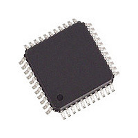
82V2081PPG8 IDT, Integrated Device Technology Inc, 82V2081PPG8 Datasheet - Page 38

82V2081PPG8
Manufacturer Part Number
82V2081PPG8
Description
Manufacturer
IDT, Integrated Device Technology Inc
Datasheet
1.82V2081PPG8.pdf
(68 pages)
Specifications of 82V2081PPG8
Number Of Transceivers
1
Screening Level
Industrial
Mounting
Surface Mount
Package Type
TQFP
Operating Temperature (min)
-40C
Operating Temperature (max)
85C
Lead Free Status / RoHS Status
Compliant
SINGLE CHANNEL T1/E1/J1 LONG HAUL/SHORT HAUL LINE INTERFACE UNIT
Table-32 TCF3: Transmitter Configuration Register 3
Table-33 TCF4: Transmitter Configuration Register 4
4.2.3
Table-34 RCF0: Receiver Configuration Register 0
RCLK_SEL
SAMP[3:0]
WDAT[6:0]
R_MD[1:0]
Symbol
Symbol
Symbol
RD_INV
R_OFF
UI[1:0]
DONE
RW
RECEIVE PATH CONTROL REGISTERS
-
-
(R/W, Address = 08H)
(R/W, Address = 09H)
(R/W, Address = 0AH)
5-4
3-0
6-0
7-5
1-0
Bit
Bit
Bit
7
4
3
2
6
7
0000000
Default
Default
Default
0000
000
00
00
0
0
0
0
0
0
These bits specify the sample address. Each UI has totally 16 samples.
Receiver power down enable
Receive data invert
Receive clock edge select (this bit is ignored in slicer mode)
Receive path decoding selection
After ‘1’ is written to this bit, a read or write operation is implemented.
This bit selects read or write operation
= 0: Write to RAM
= 1: Read from RAM
These bits specify the unit interval address. There are totally 4 unit intervals.
= 00: UI address is 0 (The most left UI)
= 01: UI address is 1
= 10: UI address is 2
= 11: UI address is 3
= 0000: Sample address is 0 (The most left sample)
= 0001: Sample address is 1
= 0010: Sample address is 2
……
= 1110: Sample address is 14
= 1111: Sample address is 15
Reserved
In Indirect Write operation, the WDAT[6:0] will be loaded to the pulse template RAM, specifying the amplitude of
the Sample.
After an Indirect Read operation, the amplitude data of the Sample in the pulse template RAM will be output to the
WDAT[6:0].
Reserved
= 0: Receiver power up
= 1: Receiver power down
= 0: Data on RD or RDP/RDN is active high
= 1: Data on RD or RDP/RDN is active low
= 0: Data on RD or RDP/RDN is updated on the rising edge of RCLK
= 1: Data on RD or RDP/RDN is updated on the falling edge of RCLK
= 00: Receive data is HDB3 (E1)/B8ZS (T1/J1) decoded and output on RD pin with single rail NRZ format
= 01: Receive data is AMI decoded and output on RD pin with single rail NRZ format
= 10: Decoder is bypassed, re-timed dual rail data with NRZ format output on RDP/RDN (dual rail mode with clock
recovery)
= 11: CDR and decoder are bypassed, slicer data with RZ format output on RDP/RDN (slicer mode)
38
Description
Description
Description
TEMPERATURE RANGES
INDUSTRIAL


