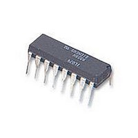
PCF8591P NXP Semiconductors, PCF8591P Datasheet - Page 10

PCF8591P
Manufacturer Part Number
PCF8591P
Description
IC, A/D AND D/A CONVERTER, 8BIT, 16-DIP
Manufacturer
NXP Semiconductors
Type
General Purposer
Specifications of PCF8591P
Number Of Channels
1
Number Of Adc's
1
Number Of Dac's
1
Adc/dac Resolution
8b
Interface Type
Serial (I2C)
Operating Supply Voltage (typ)
3.3/5V
Sample Rate
11.1KSPS
Number Of Adc Inputs
4
Number Of Dac Outputs
1
Operating Supply Voltage (max)
6V
Operating Supply Voltage (min)
2.5V
Operating Temperature (max)
85C
Operating Temperature (min)
-40C
Pin Count
16
Mounting
Through Hole
Supply Voltage Range
2.5V To 6V
Operating Temperature Range
-40°C To +85°C
Digital Ic Case Style
DIP
No. Of Pins
16
Linearity Error -
1.5LSB
Termination Type
DIP
Supply Voltage Max
8V
Input Channels Per Adc
1
Rohs Compliant
Yes
Filter Terminals
DIP
Conversion Time
90µs
Data Interface
I2C, Serial
Lead Free Status / RoHS Status
Compliant
Available stocks
Company
Part Number
Manufacturer
Quantity
Price
Company:
Part Number:
PCF8591P
Manufacturer:
SANYO
Quantity:
20 200
Company:
Part Number:
PCF8591P
Manufacturer:
NXP
Quantity:
5 510
Philips Semiconductors
7.4
The A/D converter makes use of the successive
approximation conversion technique. The on-chip D/A
converter and a high-gain comparator are used
temporarily during an A/D conversion cycle.
An A/D conversion cycle is always started after sending a
valid read mode address to a PCF8591 device. The A/D
conversion cycle is triggered at the trailing edge of the
acknowledge clock pulse and is executed while
transmitting the result of the previous conversion (see
Fig.8).
Once a conversion cycle is triggered an input voltage
sample of the selected channel is stored on the chip and is
converted to the corresponding 8-bit binary code. Samples
picked up from differential inputs are converted to an 8-bit
two’s complement code (see Figs 9 and 10).
1998 Jul 02
8-bit A/D and D/A converter
A/D conversion
Fig.8 A/D conversion sequence.
10
The conversion result is stored in the ADC data register
and awaits transmission. If the auto-increment flag is set
the next channel is selected.
The first byte transmitted in a read cycle contains the
conversion result code of the previous read cycle. After a
Power-on reset condition the first byte read is a
hexadecimal 80. The protocol of an I
shown in Chapter 8, Figs 15 and 16.
The maximum A/D conversion rate is given by the actual
speed of the I
2
C-bus.
2
Product specification
C-bus read cycle is
PCF8591


