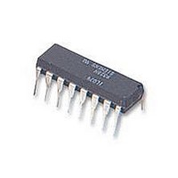
PCF8591P NXP Semiconductors, PCF8591P Datasheet - Page 12
PCF8591P
Manufacturer Part Number
PCF8591P
Description
IC, A/D AND D/A CONVERTER, 8BIT, 16-DIP
Manufacturer
NXP Semiconductors
Type
General Purposer
Specifications of PCF8591P
Number Of Channels
1
Number Of Adc's
1
Number Of Dac's
1
Adc/dac Resolution
8b
Interface Type
Serial (I2C)
Operating Supply Voltage (typ)
3.3/5V
Sample Rate
11.1KSPS
Number Of Adc Inputs
4
Number Of Dac Outputs
1
Operating Supply Voltage (max)
6V
Operating Supply Voltage (min)
2.5V
Operating Temperature (max)
85C
Operating Temperature (min)
-40C
Pin Count
16
Mounting
Through Hole
Supply Voltage Range
2.5V To 6V
Operating Temperature Range
-40°C To +85°C
Digital Ic Case Style
DIP
No. Of Pins
16
Linearity Error -
1.5LSB
Termination Type
DIP
Supply Voltage Max
8V
Input Channels Per Adc
1
Rohs Compliant
Yes
Filter Terminals
DIP
Conversion Time
90µs
Data Interface
I2C, Serial
Lead Free Status / RoHS Status
Compliant
Available stocks
Company
Part Number
Manufacturer
Quantity
Price
Company:

Part Number:
PCF8591P
Manufacturer:
SANYO
Quantity:
20 200
Company:
Part Number:
PCF8591P
Manufacturer:
NXP
Quantity:
5 510


Philips Semiconductors
7.5
For the D/A and A/D conversion either a stable external
voltage reference or the supply voltage has to be applied
to the resistor divider chain (pins V
The AGND pin has to be connected to the system analog
ground and may have a DC off-set with reference to V
A low frequency may be applied to the V
pins. This allows the use of the D/A converter as a
one-quadrant multiplier; see Chapter 15 and Fig.6.
The A/D converter may also be used as a one or two
quadrant analog divider. The analog input voltage is
divided by the reference voltage. The result is converted to
a binary code. In this application the user has to keep the
reference voltage stable during the conversion cycle.
1998 Jul 02
8-bit A/D and D/A converter
Reference voltage
REF
and AGND).
REF
and AGND
SS
.
12
7.6
An on-chip oscillator generates the clock signal required
for the A/D conversion cycle and for refreshing the
auto-zeroed buffer amplifier. When using this oscillator the
EXT pin has to be connected to V
oscillator frequency is available.
If the EXT pin is connected to V
OSC is switched to a high-impedance state allowing the
user to feed an external clock signal to OSC.
Oscillator
DD
SS
the oscillator output
. At the OSC pin the
Product specification
PCF8591
Related parts for PCF8591P
Image
Part Number
Description
Manufacturer
Datasheet
Request
R

Part Number:
Description:
NXP Semiconductors designed the LPC2420/2460 microcontroller around a 16-bit/32-bitARM7TDMI-S CPU core with real-time debug interfaces that include both JTAG andembedded trace
Manufacturer:
NXP Semiconductors
Datasheet:

Part Number:
Description:
NXP Semiconductors designed the LPC2458 microcontroller around a 16-bit/32-bitARM7TDMI-S CPU core with real-time debug interfaces that include both JTAG andembedded trace
Manufacturer:
NXP Semiconductors
Datasheet:
Part Number:
Description:
NXP Semiconductors designed the LPC2468 microcontroller around a 16-bit/32-bitARM7TDMI-S CPU core with real-time debug interfaces that include both JTAG andembedded trace
Manufacturer:
NXP Semiconductors
Datasheet:
Part Number:
Description:
NXP Semiconductors designed the LPC2470 microcontroller, powered by theARM7TDMI-S core, to be a highly integrated microcontroller for a wide range ofapplications that require advanced communications and high quality graphic displays
Manufacturer:
NXP Semiconductors
Datasheet:
Part Number:
Description:
NXP Semiconductors designed the LPC2478 microcontroller, powered by theARM7TDMI-S core, to be a highly integrated microcontroller for a wide range ofapplications that require advanced communications and high quality graphic displays
Manufacturer:
NXP Semiconductors
Datasheet:
Part Number:
Description:
The Philips Semiconductors XA (eXtended Architecture) family of 16-bit single-chip microcontrollers is powerful enough to easily handle the requirements of high performance embedded applications, yet inexpensive enough to compete in the market for hi
Manufacturer:
NXP Semiconductors
Datasheet:
Part Number:
Description:
The XA-S3 device is a member of Philips Semiconductors? XA(eXtended Architecture) family of high performance 16-bitsingle-chip microcontrollers
Manufacturer:
NXP Semiconductors
Datasheet:

Part Number:
Description:
The NXP BlueStreak LH75401/LH75411 family consists of two low-cost 16/32-bit System-on-Chip (SoC) devices
Manufacturer:
NXP Semiconductors
Datasheet:
Part Number:
Description:
The NXP LPC3130/3131 combine an 180 MHz ARM926EJ-S CPU core, high-speed USB2
Manufacturer:
NXP Semiconductors
Datasheet:
Part Number:
Description:
The NXP LPC3141 combine a 270 MHz ARM926EJ-S CPU core, High-speed USB 2
Manufacturer:
NXP Semiconductors
Part Number:
Description:
The NXP LPC3143 combine a 270 MHz ARM926EJ-S CPU core, High-speed USB 2
Manufacturer:
NXP Semiconductors

Part Number:
Description:
The NXP LPC3152 combines an 180 MHz ARM926EJ-S CPU core, High-speed USB 2
Manufacturer:
NXP Semiconductors
Part Number:
Description:
The NXP LPC3154 combines an 180 MHz ARM926EJ-S CPU core, High-speed USB 2
Manufacturer:
NXP Semiconductors

Part Number:
Description:
Standard level N-channel enhancement mode Field-Effect Transistor (FET) in a plastic package using NXP High-Performance Automotive (HPA) TrenchMOS technology
Manufacturer:
NXP Semiconductors
Datasheet: