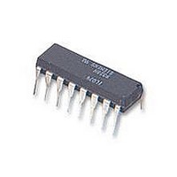
PCF8591P NXP Semiconductors, PCF8591P Datasheet - Page 17

PCF8591P
Manufacturer Part Number
PCF8591P
Description
IC, A/D AND D/A CONVERTER, 8BIT, 16-DIP
Manufacturer
NXP Semiconductors
Type
General Purposer
Specifications of PCF8591P
Number Of Channels
1
Number Of Adc's
1
Number Of Dac's
1
Adc/dac Resolution
8b
Interface Type
Serial (I2C)
Operating Supply Voltage (typ)
3.3/5V
Sample Rate
11.1KSPS
Number Of Adc Inputs
4
Number Of Dac Outputs
1
Operating Supply Voltage (max)
6V
Operating Supply Voltage (min)
2.5V
Operating Temperature (max)
85C
Operating Temperature (min)
-40C
Pin Count
16
Mounting
Through Hole
Supply Voltage Range
2.5V To 6V
Operating Temperature Range
-40°C To +85°C
Digital Ic Case Style
DIP
No. Of Pins
16
Linearity Error -
1.5LSB
Termination Type
DIP
Supply Voltage Max
8V
Input Channels Per Adc
1
Rohs Compliant
Yes
Filter Terminals
DIP
Conversion Time
90µs
Data Interface
I2C, Serial
Lead Free Status / RoHS Status
Compliant
Available stocks
Company
Part Number
Manufacturer
Quantity
Price
Company:
Part Number:
PCF8591P
Manufacturer:
SANYO
Quantity:
20 200
Company:
Part Number:
PCF8591P
Manufacturer:
NXP
Quantity:
5 510
Philips Semiconductors
11 DC CHARACTERISTICS
V
Notes
1. The power on reset circuit resets the I
2. A further extension of the range is possible, if the following conditions are fulfilled:
1998 Jul 02
Supply
V
I
V
Digital inputs/output: SCL, SDA, A0, A1, A2
V
V
I
C
I
Reference voltage inputs
V
V
I
R
Oscillator: OSC, EXT
I
f
SYMBOL
DD
L
OL
LI
LI
OSC
DD
DD
POR
IL
IH
REF
AGND
i
REF
8-bit A/D and D/A converter
V
------------------------------------- -
= 2.5 V to 6 V; V
REF
+
2
V
supply voltage (operating)
supply current
Power-on reset level
LOW level input voltage
HIGH level input voltage
leakage current
input capacitance
LOW level SDA output current V
reference voltage
analog ground voltage
input leakage current
input resistance
input leakage current
oscillator frequency
AGND
standby
operating, AOUT off
operating, AOUT active
A0, A1, A2
SCL, SDA
SS
PARAMETER
0.8V V
= 0 V; T
DD
amb
–
V
------------------------------------- -
= 40 C to 85 C unless otherwise specified.
REF
+
2
V
2
C-bus logic when V
AGND
V
f
f
note 1
V
V
V
V
pins V
SCL
SCL
I
I
I
OL
REF
REF
= V
= V
= V
= 0.4 V
= 100 kHz
= 100 kHz
> V
> V
0.4V
SS
SS
SS
REF
CONDITIONS
or V
to V
AGND
AGND
to V
and AGND
DD
DD
17
DD
; note 2
; note 2
; no load
DD
is less than V
2.5
0.8
0
0.7
3.0
V
V
0.75
250
1
250
SS
SS
MIN.
POR
+ 1.6
V
.
DD
1
125
0.45
100
TYP.
Product specification
6.0
15
250
1.0
2.0
0.3
V
+250
+1
5
V
V
+250
250
1.25
DD
DD
DD
MAX.
PCF8591
V
0.8 V
DD
V
mA
V
V
V
nA
pF
mA
V
nA
k
nA
MHz
UNIT
A
A
A


