PCF8591P NXP Semiconductors, PCF8591P Datasheet - Page 18
PCF8591P
Manufacturer Part Number
PCF8591P
Description
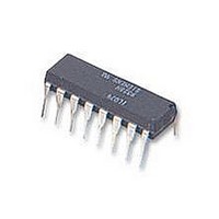
IC, A/D AND D/A CONVERTER, 8BIT, 16-DIP
Manufacturer
NXP Semiconductors
Type
General Purposer
Specifications of PCF8591P
Number Of Channels
1
Number Of Adc's
1
Number Of Dac's
1
Adc/dac Resolution
8b
Interface Type
Serial (I2C)
Operating Supply Voltage (typ)
3.3/5V
Sample Rate
11.1KSPS
Number Of Adc Inputs
4
Number Of Dac Outputs
1
Operating Supply Voltage (max)
6V
Operating Supply Voltage (min)
2.5V
Operating Temperature (max)
85C
Operating Temperature (min)
-40C
Pin Count
16
Mounting
Through Hole
Supply Voltage Range
2.5V To 6V
Operating Temperature Range
-40°C To +85°C
Digital Ic Case Style
DIP
No. Of Pins
16
Linearity Error -
1.5LSB
Termination Type
DIP
Supply Voltage Max
8V
Input Channels Per Adc
1
Rohs Compliant
Yes
Filter Terminals
DIP
Conversion Time
90µs
Data Interface
I2C, Serial
Lead Free Status / RoHS Status
Compliant
Available stocks
Company
Part Number
Manufacturer
Quantity
Price
Company:

Part Number:
PCF8591P
Manufacturer:
SANYO
Quantity:
20 200
Company:
Part Number:
PCF8591P
Manufacturer:
NXP
Quantity:
5 510


Philips Semiconductors
12 D/A CHARACTERISTICS
V
specified.
13 A/D CHARACTERISTICS
V
1998 Jul 02
Analog output
V
I
Accuracy
OS
L
G
t
f
SNRR
Analog inputs
V
I
C
C
V
V
Accuracy
OS
L
G
GS
CMRR
SNRR
t
f
SYMBOL
SYMBOL
LO
DAC
DAC
LIA
ADC
ADC
DD
DD
e
e
OA
IA
IS
ID
IA
ID
8-bit A/D and D/A converter
e
e
e
e
e
= 5.0 V; V
= 5.0 V; V
output voltage
output leakage current
offset error
linearity error
gain error
settling time
conversion rate
supply noise rejection ratio
analog input voltage
analog input leakage current
analog input capacitance
differential input capacitance
single-ended voltage
differential voltage
offset error
linearity error
gain error
small-signal gain error
common-mode rejection
ratio
supply noise rejection ratio
conversion time
sampling/conversion rate
SS
SS
= 0 V; V
= 0 V; V
PARAMETER
PARAMETER
REF
REF
= 5.0 V; V
= 5.0 V; V
AGND
AGND
no resistive load
R
AOUT disabled
T
no resistive load
to
f = 100 Hz;
V
measuring range
measuring range;
V
T
f = 100 Hz;
V
= 0 V; R
amb
amb
V
DDN
FS
DDN
L
= 0 V; R
1
i
= 10 k
2
= 16 LSB
= V
= 25 C
LSB full scale step
= 25 C
= 0.1
= 0.1
CONDITIONS
CONDITIONS
REF
L
S
= 10 k ; C
= 10 k ; T
V
V
V
PP
PP
18
AGND
L
amb
= 100 pF; T
= 40 C to +85 C unless otherwise specified.
V
V
V
V
–
------------ -
SS
SS
SS
AGND
V
2
MIN.
MIN.
FS
amb
= 40 C to +85 C unless otherwise
40
10
10
60
40
TYP.
TYP.
V
0.9
250
50
1
90
11.1
V
100
V
20
1
5
90
11.1
+V
------------- -
1.5
1.5
DD
DD
REF
Product specification
MAX.
MAX.
2
FS
V
PCF8591
DD
V
V
nA
mV
LSB
%
kHz
dB
V
nA
pF
pF
V
V
mV
LSB
%
%
dB
dB
kHz
s
s
UNIT
UNIT
Related parts for PCF8591P
Image
Part Number
Description
Manufacturer
Datasheet
Request
R

Part Number:
Description:
NXP Semiconductors designed the LPC2420/2460 microcontroller around a 16-bit/32-bitARM7TDMI-S CPU core with real-time debug interfaces that include both JTAG andembedded trace
Manufacturer:
NXP Semiconductors
Datasheet:

Part Number:
Description:
NXP Semiconductors designed the LPC2458 microcontroller around a 16-bit/32-bitARM7TDMI-S CPU core with real-time debug interfaces that include both JTAG andembedded trace
Manufacturer:
NXP Semiconductors
Datasheet:
Part Number:
Description:
NXP Semiconductors designed the LPC2468 microcontroller around a 16-bit/32-bitARM7TDMI-S CPU core with real-time debug interfaces that include both JTAG andembedded trace
Manufacturer:
NXP Semiconductors
Datasheet:
Part Number:
Description:
NXP Semiconductors designed the LPC2470 microcontroller, powered by theARM7TDMI-S core, to be a highly integrated microcontroller for a wide range ofapplications that require advanced communications and high quality graphic displays
Manufacturer:
NXP Semiconductors
Datasheet:
Part Number:
Description:
NXP Semiconductors designed the LPC2478 microcontroller, powered by theARM7TDMI-S core, to be a highly integrated microcontroller for a wide range ofapplications that require advanced communications and high quality graphic displays
Manufacturer:
NXP Semiconductors
Datasheet:
Part Number:
Description:
The Philips Semiconductors XA (eXtended Architecture) family of 16-bit single-chip microcontrollers is powerful enough to easily handle the requirements of high performance embedded applications, yet inexpensive enough to compete in the market for hi
Manufacturer:
NXP Semiconductors
Datasheet:
Part Number:
Description:
The XA-S3 device is a member of Philips Semiconductors? XA(eXtended Architecture) family of high performance 16-bitsingle-chip microcontrollers
Manufacturer:
NXP Semiconductors
Datasheet:

Part Number:
Description:
The NXP BlueStreak LH75401/LH75411 family consists of two low-cost 16/32-bit System-on-Chip (SoC) devices
Manufacturer:
NXP Semiconductors
Datasheet:
Part Number:
Description:
The NXP LPC3130/3131 combine an 180 MHz ARM926EJ-S CPU core, high-speed USB2
Manufacturer:
NXP Semiconductors
Datasheet:
Part Number:
Description:
The NXP LPC3141 combine a 270 MHz ARM926EJ-S CPU core, High-speed USB 2
Manufacturer:
NXP Semiconductors
Part Number:
Description:
The NXP LPC3143 combine a 270 MHz ARM926EJ-S CPU core, High-speed USB 2
Manufacturer:
NXP Semiconductors

Part Number:
Description:
The NXP LPC3152 combines an 180 MHz ARM926EJ-S CPU core, High-speed USB 2
Manufacturer:
NXP Semiconductors
Part Number:
Description:
The NXP LPC3154 combines an 180 MHz ARM926EJ-S CPU core, High-speed USB 2
Manufacturer:
NXP Semiconductors

Part Number:
Description:
Standard level N-channel enhancement mode Field-Effect Transistor (FET) in a plastic package using NXP High-Performance Automotive (HPA) TrenchMOS technology
Manufacturer:
NXP Semiconductors
Datasheet: