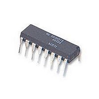
PCF8591P NXP Semiconductors, PCF8591P Datasheet - Page 8

PCF8591P
Manufacturer Part Number
PCF8591P
Description
IC, A/D AND D/A CONVERTER, 8BIT, 16-DIP
Manufacturer
NXP Semiconductors
Type
General Purposer
Specifications of PCF8591P
Number Of Channels
1
Number Of Adc's
1
Number Of Dac's
1
Adc/dac Resolution
8b
Interface Type
Serial (I2C)
Operating Supply Voltage (typ)
3.3/5V
Sample Rate
11.1KSPS
Number Of Adc Inputs
4
Number Of Dac Outputs
1
Operating Supply Voltage (max)
6V
Operating Supply Voltage (min)
2.5V
Operating Temperature (max)
85C
Operating Temperature (min)
-40C
Pin Count
16
Mounting
Through Hole
Supply Voltage Range
2.5V To 6V
Operating Temperature Range
-40°C To +85°C
Digital Ic Case Style
DIP
No. Of Pins
16
Linearity Error -
1.5LSB
Termination Type
DIP
Supply Voltage Max
8V
Input Channels Per Adc
1
Rohs Compliant
Yes
Filter Terminals
DIP
Conversion Time
90µs
Data Interface
I2C, Serial
Lead Free Status / RoHS Status
Compliant
Available stocks
Company
Part Number
Manufacturer
Quantity
Price
Company:
Part Number:
PCF8591P
Manufacturer:
SANYO
Quantity:
20 200
Company:
Part Number:
PCF8591P
Manufacturer:
NXP
Quantity:
5 510
Philips Semiconductors
7.3
The third byte sent to a PCF8591 device is stored in the
DAC data register and is converted to the corresponding
analog voltage using the on-chip D/A converter. This D/A
converter consists of a resistor divider chain connected to
the external reference voltage with 256 taps and selection
switches. The tap-decoder switches one of these taps to
the DAC output line (see Fig.5).
The analog output voltage is buffered by an auto-zeroed
unity gain amplifier. This buffer amplifier may be switched
on or off by setting the analog output enable flag of the
control register. In the active state the output voltage is
held until a further data byte is sent.
1998 Jul 02
8-bit A/D and D/A converter
D/A conversion
Fig.5 DAC resistor divider chain.
8
The on-chip D/A converter is also used for successive
approximation A/D conversion. In order to release the
DAC for an A/D conversion cycle the unity gain amplifier is
equipped with a track and hold circuit. This circuit holds the
output voltage while executing the A/D conversion.
The output voltage supplied to the analog output AOUT is
given by the formula shown in Fig.6. The waveforms of a
D/A conversion sequence are shown in Fig.7.
Product specification
PCF8591


