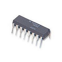
PCF8591P NXP Semiconductors, PCF8591P Datasheet - Page 20

PCF8591P
Manufacturer Part Number
PCF8591P
Description
IC, A/D AND D/A CONVERTER, 8BIT, 16-DIP
Manufacturer
NXP Semiconductors
Type
General Purposer
Specifications of PCF8591P
Number Of Channels
1
Number Of Adc's
1
Number Of Dac's
1
Adc/dac Resolution
8b
Interface Type
Serial (I2C)
Operating Supply Voltage (typ)
3.3/5V
Sample Rate
11.1KSPS
Number Of Adc Inputs
4
Number Of Dac Outputs
1
Operating Supply Voltage (max)
6V
Operating Supply Voltage (min)
2.5V
Operating Temperature (max)
85C
Operating Temperature (min)
-40C
Pin Count
16
Mounting
Through Hole
Supply Voltage Range
2.5V To 6V
Operating Temperature Range
-40°C To +85°C
Digital Ic Case Style
DIP
No. Of Pins
16
Linearity Error -
1.5LSB
Termination Type
DIP
Supply Voltage Max
8V
Input Channels Per Adc
1
Rohs Compliant
Yes
Filter Terminals
DIP
Conversion Time
90µs
Data Interface
I2C, Serial
Lead Free Status / RoHS Status
Compliant
Available stocks
Company
Part Number
Manufacturer
Quantity
Price
Company:
Part Number:
PCF8591P
Manufacturer:
SANYO
Quantity:
20 200
Company:
Part Number:
PCF8591P
Manufacturer:
NXP
Quantity:
5 510
Philips Semiconductors
14 AC CHARACTERISTICS
All timing values are valid within the operating supply voltage and ambient temperature range and reference to V
V
Note
1. A detailed description of the I
1998 Jul 02
I
f
t
t
t
t
t
t
t
t
t
t
t
t
handbook, full pagewidth
2
SCL
SP
BUF
SU;STA
HD;STA
LOW
HIGH
r
f
SU;DAT
HD;DAT
VD;DAT
SU;STO
IH
SYMBOL
C-bus timing (see Fig.19; note 1)
8-bit A/D and D/A converter
PROTOCOL
SDA
SCL
with an input voltage swing of V
use it” . This brochure may be ordered using the code 9398 393 40011.
SCL clock frequency
tolerable spike width on bus
bus free time
START condition set-up time
START condition hold time
SCL LOW time
SCL HIGH time
SCL and SDA rise time
SCL and SDA fall time
data set-up time
data hold time
SCL LOW-to-data out valid
STOP condition set-up time
t
SU;STA
t
BUF
CONDITION
START
(S)
t HD;STA
Fig.19 I
t
LOW
2
2
C-bus timing diagram; rise and fall times refer to V
C-bus specification, with applications, is given in brochure “The I
r t
SS
BIT 7
MSB
(A7)
PARAMETER
to V
t HIGH
DD
.
t
t
SU;DAT
f
1 / f SCL
BIT 6
(A6)
20
t
HD;DAT
(R/W)
BIT 0
LSB
4.7
4.7
4.0
4.7
4.0
250
0
4.0
t
VD;DAT
MIN.
ACKNOWLEDGE
IL
and V
(A)
TYP.
MBD820
IH
.
Product specification
100
100
1.0
0.3
3.4
2
CONDITION
C-bus and how to
MAX.
STOP
PCF8591
(P)
t SU;STO
kHz
ns
ns
ns
s
s
s
s
s
s
s
s
s
UNIT
IL
and


