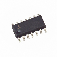
X1228S14IZ Intersil, X1228S14IZ Datasheet - Page 5

X1228S14IZ
Manufacturer Part Number
X1228S14IZ
Description
IC RTC/CAL/SUP/ALRM 4K EE 14SOIC
Manufacturer
Intersil
Type
Clock/Calendar/EEPROMr
Datasheet
1.X1228S14-2.7A.pdf
(29 pages)
Specifications of X1228S14IZ
Memory Size
4K (512 x 8)
Time Format
HH:MM:SS (12/24 hr)
Date Format
YY-MM-DD-dd
Interface
I²C, 2-Wire Serial
Voltage - Supply
2.7 V ~ 5.5 V
Operating Temperature
-40°C ~ 85°C
Mounting Type
Surface Mount
Package / Case
14-SOIC (3.9mm Width), 14-SOL
Lead Free Status / RoHS Status
Lead free / RoHS Compliant
Available stocks
Company
Part Number
Manufacturer
Quantity
Price
Company:
Part Number:
X1228S14IZ
Manufacturer:
NXP
Quantity:
906
Part Number:
X1228S14IZ-2.7A
Manufacturer:
INTERSIL
Quantity:
20 000
Notes: (1) The device enters the Active state after any start, and remains active: for 9 clock cycles if the Device Select Bits in the Slave Address
Capacitance T
Notes: (1) This parameter is not 100% tested.
AC CHARACTERISTICS
AC Test Conditions
Figure 18. Standard Output Load for testing the device with V
Input Pulse Levels
Input Rise and Fall Times
Input and Output Timing
Levels
Output Load
Symbol
C
Equivalent AC Output Load Circuit for V
C
OUT
IN
(2) The device enters the Program state 200nS after a stop ending a write operation and continues for t
(3) The device goes into the Timekeeping state 200nS after any stop, except those that initiate a nonvolatile write cycle; t
(4) For reference only and not tested.
(5) V
(6) V
(7) V
(8) V
(9) V
(10) V
(11) I
(12) I
(13) Threshold voltages based on the higher of Vcc or Vback.
(14) Using recommended crystal and oscillator network applied to X1 and X2 (25°C).
(15) Typical values are for T
(2) The input capacitance between x1 and x2 pins can be varied between 5pF and 19.75pF by using analog trimming registers
(1)
(1)
SDA
that initiates a nonvolatile write cycle; or 9 clock cycles after any start that is not followed by the correct Device Select Bits in the Slave
Address Byte.
Byte are incorrect or until 200nS after a stop ending a read or write operation.
OL
OH
IL
CC
BACK
SDA
SDA
SDA
= V
= 3.0mA at 5.5V, 1.5mA at 2.7V
= -1.0mA at 5.5V, -0.4mA at 2.7V
= 0V
Output Capacitance (SDA, PHZ/IRQ, RESET)
Input Capacitance (SCL)
= V
=V
= GND or V
A
CC
= 0V
= 25°C, f = 1.0 MHz, V
SCL
SCL
x 0.1, V
=V
5.0V
=V
BACK
CC
CC
IH
, Others = GND or V
1533Ω
100pF
, Others = GND or V
, V
= V
5
SCL
A
CC
= 25°C
= GND or V
x 0.9, f
V
10ns
V
Standard Output Load
Parameter
CC
CC
For V
and I
SCL
x 0.1 to V
x 0.5
OL
OL
CC
= 400kHz
CC
CC
= 0.4V
= 3 mA
BACK
CC
, V
= 5V
RESET
= 5V
CC
x 0.9
= V
CC
X1228
or GND
PHZ/IRQ
CC
Max.
10
10
= 5.0V
5.0V
Units
pF
pF
1316Ω
806Ω
WC
.
100pF
Test Conditions
V
V
OUT
IN
= 0V
= 0V
WC
after a stop
May 18, 2006
FN8100.4


