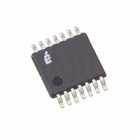
X1288V14T1 Intersil, X1288V14T1 Datasheet - Page 14

X1288V14T1
Manufacturer Part Number
X1288V14T1
Description
IC RTC/CAL/CPU SUP EE 14-TSSOP
Manufacturer
Intersil
Type
Clock/Calendar/Supervisor/EEPROMr
Datasheet
1.X1288S16.pdf
(27 pages)
Specifications of X1288V14T1
Memory Size
256K (32K x 8)
Time Format
HH:MM:SS:hh (12/24 hr)
Date Format
YY-MM-DD-dd
Interface
I²C, 2-Wire Serial
Voltage - Supply
4.5 V ~ 5.5 V
Operating Temperature
-40°C ~ 85°C
Mounting Type
Surface Mount
Package / Case
14-TSSOP
Lead Free Status / RoHS Status
Contains lead / RoHS non-compliant
Table 6. Digital Trimming Registers
Analog Trimming Register (ATR) (Non-volatile)
Six analog trimming Bits from ATR5 to ATR0 are pro-
vided to adjust the on-chip loading capacitance range.
The on-chip load capacitance ranges from 3.25pF to
18.75pF. Each bit has a different weight for capacitance
adjustment. Using a Citizen CFS-206 crystal with differ-
ent ATR bit combinations provides an estimated ppm
range from +116ppm to -37ppm to the nominal fre-
quency compensation. The combination of digital and
analog trimming can give up to +146ppm adjustment.
The on-chip capacitance can be calculated as follows:
C
Note that the ATR values are in two’s complement, with
ATR(000000) = 11.0pF, so the entire range runs from
3.25pF to 18.75pF in 0.25pF steps.
The values calculated above are typical, and total load
capacitance seen by the crystal will include approxi-
mately 2pF of package and board capacitance in addi-
tion to the ATR value.
See Application section and Intersil’s Application Note
AN154 for more information.
WRITING TO THE CLOCK/CONTROL REGISTERS
Changing any of the nonvolatile bits of the clock/
control register requires the following steps:
– Write a 02h to the Status Register to set the Write
– Write a 06h to the Status Register to set both the Reg-
– Write one to 8 bytes to the Clock/Control Registers
ATR
DTR2
Enable Latch (WEL). This is a volatile operation, so
there is no delay after the write. (Operation preceeded
by a start and ended with a stop).
ister Write Enable Latch (RWEL) and the WEL bit. This
is also a volatile cycle. The zeros in the data byte are
required. (Operation preceeded by a start and ended
with a stop).
with the desired clock, alarm, or control data. This
sequence starts with a start bit, requires a slave byte of
“11011110” and an address within the CCR and is ter-
0
0
0
0
1
1
1
1
= [(ATR value, decimal) x 0.25pF] + 11.0pF
DTR Register
DTR1
0
1
0
1
0
1
0
1
DTR0
0
0
1
1
0
0
1
1
14
Estimated frequency
PPM
+10
+20
+30
-10
-20
-30
0
0
X1288
– Writing all zeros to the status register resets both the
– A read operation occurring between any of the previ-
POWER-ON RESET
Application of power to the X1288 activates a Power-on
Reset Circuit that pulls the RESET pin active. This signal
provides several benefits.
– It prevents the system microprocessor from starting to
– It prevents the processor from operating prior to stabili-
– It allows time for an FPGA to download its configura-
– It prevents communication to the EEPROM, greatly
When V
typically, 250ms the circuit releases RESET, allowing the
system to begin operation. Recommended V
is between 0.2V/ms and 50V/ms.
WATCHDOG TIMER OPERATION
The watchdog timer is selectable. By writing a value to
WD1 and WD0, the watchdog timer can be set to 3 differ-
ent time out periods or off. When the Watchdog timer is
set to off, the watchdog circuit is configured for low power
operation.
Watchdog Timer Restart
The Watchdog Timer is started by a falling edge of SDA
when the SCL line is high and followed by a stop bit. The
start signal restarts the watchdog timer counter, resetting
the period of the counter back to the maximum. If another
start fails to be detected prior to the watchdog timer expi-
ration, then the RESET pin becomes active. In the event
that the start signal occurs during a reset time out period,
the start will have no effect. When using a single START
to refresh watchdog timer, a STOP bit should be followed
to reset the device back to stand-by mode.
minated by a stop bit. A write to the CCR changes
EEPROM values so these initiate a nonvolatile write
cycle and will take up to 10ms to complete. Writes to
undefined areas have no effect. The RWEL bit is reset
by the completion of a nonvolatile write cycle, so the
sequence must be repeated to again initiate another
change to the CCR contents. If the sequence is not
completed for any reason (by sending an incorrect
number of bits or sending a start instead of a stop, for
example) the RWEL bit is not reset and the device
remains in an active mode.
WEL and RWEL bits.
ous operations will not interrupt the register write oper-
ation.
operate with insufficient voltage.
zation of the oscillator.
tion prior to initialization of the circuit.
reducing the likelihood of data corruption on power-up.
CC
exceeds the device V
TRIP
threshold value for
CC
April 14, 2006
slew rate
FN8102.3


