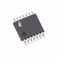
X1288V14T1 Intersil, X1288V14T1 Datasheet - Page 3

X1288V14T1
Manufacturer Part Number
X1288V14T1
Description
IC RTC/CAL/CPU SUP EE 14-TSSOP
Manufacturer
Intersil
Type
Clock/Calendar/Supervisor/EEPROMr
Datasheet
1.X1288S16.pdf
(27 pages)
Specifications of X1288V14T1
Memory Size
256K (32K x 8)
Time Format
HH:MM:SS:hh (12/24 hr)
Date Format
YY-MM-DD-dd
Interface
I²C, 2-Wire Serial
Voltage - Supply
4.5 V ~ 5.5 V
Operating Temperature
-40°C ~ 85°C
Mounting Type
Surface Mount
Package / Case
14-TSSOP
Lead Free Status / RoHS Status
Contains lead / RoHS non-compliant
PIN ASSIGNMENTS
SOIC
Pin Number
10
14
15
16
1
2
7
8
9
TSSOP
12
13
14
1
2
6
7
8
9
PHZ/IRQ
Symbol
RESET
V
SDA
SCL
V
V
BACK
X1
X2
CC
SS
3
X1. The X1 pin is the input of an inverting amplifier. An external 32.768kHz quartz
crystal is used with the X1288 to supply a timebase for the real time clock. The
recommended crystal is a Citizen CFS206-32.768KDZF. Internal compensation circuitry is
included to form a complete oscillator circuit. Care should be taken in the placement of the
crystal and the layout of the circuit. Plenty of ground plane around the device and short
traces to X1 are highly recommended. See Application section for more information.
X2. The X2 pin is the output of an inverting amplifier. An external 32.768kHz quartz
crystal is used with the X1288 to supply a timebase for the real time clock. The
recommended crystal is a Citizen CFS206-32.768KDZF. Internal compensation circuitry is
included to form a complete oscillator circuit. Care should be taken in the placement of the
crystal and the layout of the circuit. Plenty of ground plane around the device and short
traces to X2 are highly recommended. See Application section for more information.
RESET Output – RESET. This is a reset signal output. This signal notifies a host
processor that the watchdog time period has expired or that the voltage has dropped
below a fixed V
value for the pullup resistor is 5kΩ. If unused, tie to ground.
V
Serial Data (SDA). SDA is a bidirectional pin used to transfer data into and out of the
device. It has an open drain output and may be wire ORed with other open drain or open
collector outputs. The input buffer is always active (not gated).
An open drain output requires the use of a pull-up resistor. The output circuitry controls
the fall time of the output signal with the use of a slope controlled pull-down. The circuit
is designed for 400kHz 2-wire interface speed.
Serial Clock (SCL). The SCL input is used to clock all data into and out of the device.
The input buffer on this pin is always active (not gated).
Programmable Frequency/Interrupt Output – PHZ/IRQ. This is either an output from
the internal oscillator or an interrupt signal output. It is a CMOS output.
When used as frequency output, this signal has a frequency of 32.768kHz, 100Hz, 1Hz
or inactive.
When used as interrupt output, this signal notifies a host processor that an alarm has
occurred and an action is required. It is an active LOW output.
The control bits for this function are FO1 and FO0 and are found in address 0011h of
the Clock Control Memory map. See “Programmable Frequency Output Bits - FO1,
FO0” on page 13.
V
power to the device in the event the V
battery, a Supercap or tied to ground if not used.
V
SS
BACK
CC
.
.
. This input provides a backup supply voltage to the device. V
TRIP
threshold. It is an open drain active LOW output. Recommended
X1288
Brief Description
CC
supply fails. This pin can be connected to a
BACK
supplies
April 14, 2006
FN8102.3


