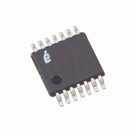
X1288V14T1 Intersil, X1288V14T1 Datasheet - Page 18

X1288V14T1
Manufacturer Part Number
X1288V14T1
Description
IC RTC/CAL/CPU SUP EE 14-TSSOP
Manufacturer
Intersil
Type
Clock/Calendar/Supervisor/EEPROMr
Datasheet
1.X1288S16.pdf
(27 pages)
Specifications of X1288V14T1
Memory Size
256K (32K x 8)
Time Format
HH:MM:SS:hh (12/24 hr)
Date Format
YY-MM-DD-dd
Interface
I²C, 2-Wire Serial
Voltage - Supply
4.5 V ~ 5.5 V
Operating Temperature
-40°C ~ 85°C
Mounting Type
Surface Mount
Package / Case
14-TSSOP
Lead Free Status / RoHS Status
Contains lead / RoHS non-compliant
.
SERIAL COMMUNICATION
Interface Conventions
The device supports a bidirectional bus oriented proto-
col. The protocol defines any device that sends data
onto the bus as a transmitter, and the receiving device
as the receiver. The device controlling the transfer is
called the master and the device being controlled is
called the slave. The master always initiates data
transfers, and provides the clock for both transmit and
receive operations. Therefore, the devices in this fam-
ily operate as slaves in all applications.
Clock and Data
Data states on the SDA line can change only during
SCL LOW. SDA state changes during SCL HIGH are
reserved for indicating start and stop conditions. See
Figure 8.
Start Condition
All commands are preceded by the start condition,
which is a HIGH to LOW transition of SDA when SCL
is HIGH. The device continuously monitors the SDA
and SCL lines for the start condition and will not
respond to any command until this condition has been
met. See Figure 9.
Stop Condition
All communications must be terminated by a stop
condition, which is a LOW to HIGH transition of SDA
when SCL is HIGH. The stop condition is also used to
FIGURE 13. WRITING 30 BYTES TO A 128-BYTE MEMORY PAGE STARTING AT ADDRESS 105
7 Bytes
Signals from
the Master
SDA Bus
Signals From
The Slave
Address
= 6
18
Address Pointer
Ends Here
Addr = 7
S
a
t
r
t
1
FIGURE 12. BYTE WRITE SEQUENCE
Address
Slave
1
1
1
0
A
C
K
X1288
0
Address 1
Word
place the device into the Standby power mode after a
read sequence. A stop condition can only be issued
after the transmitting device has released the bus. See
Figure 9.
Acknowledge
Acknowledge is a software convention used to indi-
cate successful data transfer. The transmitting device,
either master or slave, will release the bus after trans-
mitting eight bits. During the ninth clock cycle, the
receiver will pull the SDA line LOW to acknowledge
that it received the eight bits of data. Refer to Figure 10.
The device will respond with an acknowledge after rec-
ognition of a start condition and if the correct Device
Identifier and Select bits are contained in the Slave
Address Byte. If a write operation is selected, the device
will respond with an acknowledge after the receipt of
each subsequent eight bit word. The device will acknowl-
edge all incoming data and address bytes, except for:
– The Slave Address Byte when the Device Identifier
– All Data Bytes of a write when the WEL in the Write
– The 2nd Data Byte of a Status Register Write Oper-
In the read mode, the device will transmit eight bits of
data, release the SDA line, then monitor the line for an
acknowledge. If an acknowledge is detected and no
stop condition is generated by the master, the device
and/or Select bits are incorrect
Protect Register is LOW
ation (only 1 data byte is allowed)
Address
A
C
K
105
Address 0
Word
A
C
K
23 Bytes
Data
Address
A
C
K
127
S
o
p
t
April 14, 2006
FN8102.3


