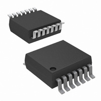
ISL22349UFV14Z-TK Intersil, ISL22349UFV14Z-TK Datasheet

ISL22349UFV14Z-TK
Specifications of ISL22349UFV14Z-TK
Related parts for ISL22349UFV14Z-TK
ISL22349UFV14Z-TK Summary of contents
Page 1
... Ordering Information PART NUMBER PART (Note) MARKING ISL22349UFV14Z* 22349 UFVZ ISL22349WFV14Z* 22349 WFVZ *Add “-TK” suffix for tape and reel. Please refer to TB347 for details on reel specifications. NOTE: These Intersil Pb-free plastic packaged products employ special Pb-free material sets, molding compounds/die attach materials, and 100% matte tin plate plus anneal (e3 termination finish, which is RoHS compliant and compatible with both SnPb and Pb-free soldering operations) ...
Page 2
Block Diagram SCL SDA A0 INTERFACE A1 A2 SHDN Pin Descriptions TSSOP PIN SYMBOL 1 RW3 SCL 4 SDA 5 GND 6 RW2 7 RW1 ...
Page 3
... ISL22349 Thermal Information Thermal Resistance (Typical, Note TSSOP package . . . . . . . . . . . . . . . . . . . . . . + 0.3 CC Max Junction Temperature (Plastic Package Pb-Free Reflow Profile .see link below http://www.intersil.com/pbfree/Pb-FreeReflow.asp CC Recommended Operating Conditions Ambient Temperature . . . . . . . . . . . . . . . . . . . . . . .-40°C to +125°C V Voltage for DCP Operation . . . . . . . . . . . . . . . . . . 2.7V to 5.5V CC Wiper Current . . . . . . . . . . . . . . . . . . . . . . . . . . . . . . . -3mA to 3mA Power Rating ...
Page 4
Operating Specifications Over the recommended operating conditions unless otherwise specified. SYMBOL PARAMETER I V Supply Current (volatile CC1 CC write/read) V Supply Current (volatile CC write/read, non-volatile read Supply Current (non-volatile CC2 CC write/read) V Supply Current (non-volatile ...
Page 5
Operating Specifications Over the recommended operating conditions unless otherwise specified. (Continued) SYMBOL PARAMETER SERIAL INTERFACE SPECS V A2, A1, A0, SHDN, SDA, and SCL IL Input Buffer LOW Voltage V A2, A1, A0, SHDN, SDA, and SCL IH Input Buffer ...
Page 6
Operating Specifications Over the recommended operating conditions unless otherwise specified. (Continued) SYMBOL PARAMETER t A2, A1 and A0 Setup Time SU:A t A2, A1 and A0 Hold Time HD:A NOTES: 3. Typical values are for T = +25°C and 3.3V ...
Page 7
Typical Performance Curves 100 V = 3.3V +125° 3.3V +20° TAP POSITION (DECIMAL) FIGURE 1. WIPER RESISTANCE vs ...
Page 8
Typical Performance Curves 1 2.7V CC 0.5 0.0 -0 5.5V CC -1.0 -40 - TEMPERATURE (°C) FIGURE 7. END-TO-END R % CHANGE vs TOTAL TEMPERATURE SIGNAL AT WIPER (WIPER UNLOADED) FIGURE 9. MIDSCALE ...
Page 9
SERIAL CLOCK (SCL) 2 This is the serial clock input of the I C serial interface. SCL requires an external pull-up resistor, since open drain input. DEVICE ADDRESS (A2 - A0) The address inputs are used to ...
Page 10
Shutdown Mode The device can be put in Shutdown mode either by pulling the SHDN pin to GND or setting the SHDN bit in the ACR register to 0. The truth table for Shutdown mode is in Table 3. TABLE ...
Page 11
SCL FROM MASTER SDA OUTPUT FROM TRANSMITTER HIGH IMPEDANCE SDA OUTPUT FROM RECEIVER START FIGURE 13. ACKNOWLEDGE RESPONSE FROM RECEIVER SIGNALS FROM THE MASTER SIGNAL AT SDA SIGNALS FROM THE SLAVE S SIGNALS T FROM THE A IDENTIFICATION MASTER R ...
Page 12
Write Operation A Write operation requires a START condition, followed by a valid Identification Byte, a valid Address Byte, a Data Byte, and a STOP condition. After each of the three bytes, the ISL22349 responds with an ACK. At this ...
Page 13
... Accordingly, the reader is cautioned to verify that data sheets are current before placing orders. Information furnished by Intersil is believed to be accurate and reliable. However, no responsibility is assumed by Intersil or its subsidiaries for its use; nor for any infringements of patents or other rights of third parties which may result from its use ...


