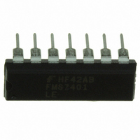
FMS7401LEN14 Fairchild Semiconductor, FMS7401LEN14 Datasheet - Page 36

FMS7401LEN14
Manufacturer Part Number
FMS7401LEN14
Description
IC CTRLR POWER DGTL EEPROM 14DIP
Manufacturer
Fairchild Semiconductor
Datasheet
1.FMS7401LVN.pdf
(81 pages)
Specifications of FMS7401LEN14
Applications
Digital Power Controller
Core Processor
8-Bit
Program Memory Type
EEPROM (1 kB)
Ram Size
64 x 8
Number Of I /o
8
Voltage - Supply
2.7 V ~ 3.6 V
Operating Temperature
-40°C ~ 85°C
Mounting Type
Through Hole
Package / Case
14-DIP (0.300", 7.62mm)
Output Current
5 mA
Input Voltage
2.7 V to 3.6 V
Switching Frequency
2 MHz
Operating Temperature Range
- 40 C to + 85 C
Mounting Style
Through Hole
Lead Free Status / RoHS Status
Lead free / RoHS Compliant
Interface
-
Controller Series
-
Lead Free Status / Rohs Status
Lead free / RoHS Compliant
Other names
FMS7401LEN14_NL
FMS7401LEN14_NL
FMS7401LEN14_NL
Available stocks
Company
Part Number
Manufacturer
Quantity
Price
Company:
Part Number:
FMS7401LEN14
Manufacturer:
Rohm
Quantity:
21 626
FMS7401L
PRODUCT SPECIFICATION
pletes, will dictate the device’s I/O attribute for the next PWM cycle. When reading the T1BOUT, the value reported will be the
last value written by software and may not necessarily reflect the device’s I/O attribute for the current PWM cycle.
Bit 4 (T1C0) of the T1CNTRL register has two functions depending on Timer 1’s selected operating mode. In PWM Mode,
when T1C0=1, the TMR1 circuit becomes enabled and begins to increment from its initial 0x000 state; otherwise, the TMR1
counter is stopped and reinitialized. Software may disable the Timer 1 circuit at any time; however, the TMR1 counter and
PWM outputs will not be disabled until the current PWM cycle completes. Software should monitor the T1C0 bit to determine
when the PWM cycle ends and Timer 1 circuit actually disabled. In Input Capture Mode, the T1C0 bit is one of the TMR1
overflow (a transition from 0xFFF to 0x000) pending flags used to trigger the Timer 1 Circuit’s hardware interrupt if the inter-
rupt is enabled. In order for software to properly monitor the TMR1 overflows, the T1C0 bit must be cleared before the next
TMR1 overflow.
Bit 3 (T1PND) of the T1CNTRL register has two functions depending on Timer 1’s selected operating mode. In either operat-
ing modes, the T1PND bit is one of the Timer 1 Circuit’s hardware interrupt pending flags if the interrupt is enabled. In PWM
Mode, the T1PND bit is triggered by a TMR1 overflow (a transition from the T1RA count to 0x000). However, in Input Cap-
ture Mode, the T1PND bit is triggered by the capture of the current TMR1 value by the rising or falling edge of the T1HS2
(G5) input port. In order for software to properly monitor the pending flag, the T1PND bit must be cleared before the next
TMR1 overflow or capture.
Bit 2 of the T1CNTRL register is the Timer 1’s microcontroller hardware interrupt enable (T1EN) bit. If set, hardware inter-
6
rupts are enabled and trigger by the T1PND and/or T1C0 pending flags depending on Timer 1’s operating mode.
If in PWM
Mode, the hardware interrupt is triggered only by the T1PND bit. If in Input Capture Mode, the T1PND and T1C0 bits are log-
ically-ORed together. As long as a Timer 1 pending flag is set, the hardware interrupt will continue to execute software’s Timer
7
1 interrupt service routine until the pending flag is cleared.
The SBIT or RBIT instructions may be used to either set or clear one of the T1CNTRL register bits, like the T1EN bit. The
SBIT and RBIT instructions both take two instruction clock cycles to complete their execution. In the first cycle, all register
bits are automatically read to obtain their most current value. In the second cycle, the bit to be set/cleared is given its new value
and all bits are then re-written to the register. Using the SBIT/RBIT instruction to set/clear an enable bit with a pending flag in
the same register may cause a potential hazard. Software may inadvertently clear a recently triggered pending flag if the trigger
happened during the second phase of the SBIT/RBIT instruction execution. To avoid this condition, the LD instruction must be
used to set or clear the interrupt enable bits. The Timer 1 circuit is designed such that software may not trigger a pending flag
by writing a 1 to the T1PND and T1C0 (if in Input Capture Mode) bits, they may only be cleared. The action of writing a 1 to a
T1PND and T1C0 register bits holds the current bit values. The action of writing a 0 to the T1PND and T1C0 register bits
clears the bit values. Therefore, if Timer 1 is configured for a rising edge triggered input capture mode with outputs enabled
and software is to enable interrupts without interrupting the pending flags, the “LD T1CNTRL, #0BDH” instruction should be
used. The T1EN bit will be set to 1 without clearing T1PND and/or T1C0.
36
REV. 1.0.3 1/24/05


