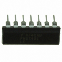
FMS7401LEN14 Fairchild Semiconductor, FMS7401LEN14 Datasheet - Page 43

FMS7401LEN14
Manufacturer Part Number
FMS7401LEN14
Description
IC CTRLR POWER DGTL EEPROM 14DIP
Manufacturer
Fairchild Semiconductor
Datasheet
1.FMS7401LVN.pdf
(81 pages)
Specifications of FMS7401LEN14
Applications
Digital Power Controller
Core Processor
8-Bit
Program Memory Type
EEPROM (1 kB)
Ram Size
64 x 8
Number Of I /o
8
Voltage - Supply
2.7 V ~ 3.6 V
Operating Temperature
-40°C ~ 85°C
Mounting Type
Through Hole
Package / Case
14-DIP (0.300", 7.62mm)
Output Current
5 mA
Input Voltage
2.7 V to 3.6 V
Switching Frequency
2 MHz
Operating Temperature Range
- 40 C to + 85 C
Mounting Style
Through Hole
Lead Free Status / RoHS Status
Lead free / RoHS Compliant
Interface
-
Controller Series
-
Lead Free Status / Rohs Status
Lead free / RoHS Compliant
Other names
FMS7401LEN14_NL
FMS7401LEN14_NL
FMS7401LEN14_NL
Available stocks
Company
Part Number
Manufacturer
Quantity
Price
Company:
Part Number:
FMS7401LEN14
Manufacturer:
Rohm
Quantity:
21 626
8
The eight I/O pins (six on the 8-pin package option) are bi-directional (see
vidually configured by software to operate as high-impedance inputs, as inputs with weak pull-up, or as push-pull outputs. The
operating state is determined by the contents of the corresponding bits in the data and configuration registers. Each bi-direc-
tional I/O pin can be used for general purpose I/O, or in some cases, for a specific alternate function determined by the on-chip
hardware.
8.1
The I/O pins (G0–G7) have three memory mapped port registers associated with the I/O circuitry: a Port Configuration
(PORTGC), Port Data (PORTGD) and Port Input (PORTGP) register.
puts. A pin may be configured as an input by writing a 0 or as an output by writing a 1 to its corresponding PORTGC bit. If a
pin is configured as an output, its PORTGD bit represents the state of the pin (1 = logic high, 0 = logic low). If the pin is con-
figured as an input, its PORTGD bit selects whether the pin is a weak pull-up or a high-impedance input.
details of the port configuration options. The port configuration and data registers can both be read from or written to. Reading
PORTGP returns the value of the port pins regardless of how the pins are configured. Since this device supports MIW, all input
ports have Schmitt triggers.
Upon power-up, the PORTGC and PORTGD registers are initialized to 0x00. However, the G0/T1HS1 and G5/T1HS2 pins
may be defaulted to the different I/O configurations defined by the default I/O configuration bits of the Initialization Register 4.
Refer to
Table 20. I/O Register Bit Assignments
Table 21. I/O Configuration Options
1. Refer to
2. Available only on the 14-pin package option.
REV. 1.0.3 1/24/05
PRODUCT SPECIFICATION
I/O Ports
Bit 7
G7
I/O Registers
Table 30
Table 29
2
PORTGC Bit
0
0
1
1
of the
in the
Device Memory
Bit 6
G6
Device Memory
GXPULLEN
2
GXBUFEN
GXOUT
GXIN
PORTGC, PORTGD, PORTGD Registers (addr. 0xB3, 0xB2, 0xB4)
section of the datasheet for the detailed memory map.
Bit 5
G5
section of the datasheet for details.
PORTGD Bit
Figure 14. PORTGD Logic Diagram
0
1
0
1
Bit 4
G4
Port Pin Configuration
High-impedance input (tri-state input)
Input with pull-up (weak one input)
Push-pull zero output
Push-pull one output
1
Bit 3
PORTGC is used to configure the pins as inputs or out-
G3
Figure
14). The bi-directional I/O pins can be indi-
Bit 2
G2
GX
Bit 1
G1
Table 20
provides
FMS7401L
Bit 0
G0
43


