Z8018010PSG Zilog, Z8018010PSG Datasheet - Page 9
Z8018010PSG
Manufacturer Part Number
Z8018010PSG
Description
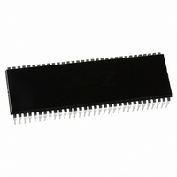
IC 10MHZ Z180 CMOS ENH MPU 64DIP
Manufacturer
Zilog
Specifications of Z8018010PSG
Processor Type
Z180
Features
8-Bit, Enhanced Z80 Megacell
Speed
10MHz
Voltage
5V
Mounting Type
Through Hole
Package / Case
64-DIP (0.750", 19.05mm)
Processor Series
Z8018xx
Core
Z80
Data Bus Width
8 bit
Maximum Clock Frequency
10 MHz
Number Of Timers
2
Operating Supply Voltage
0 V to 5 V
Maximum Operating Temperature
+ 70 C
Mounting Style
Through Hole
Minimum Operating Temperature
0 C
Core Size
8bit
Cpu Speed
10MHz
Digital Ic Case Style
DIP
No. Of Pins
64
Supply Voltage Range
4.5V To 5.5V
Operating Temperature Range
0°C To +70°C
Svhc
No SVHC (18-Jun-2010)
Base Number
8018010
Rohs Compliant
Yes
Clock Frequency
10MHz
Lead Free Status / RoHS Status
Lead free / RoHS Compliant
Other names
269-3889
Z8018010PSG
Z8018010PSG
Available stocks
Company
Part Number
Manufacturer
Quantity
Price
Company:

Part Number:
Z8018010PSG
Manufacturer:
Zilog
Quantity:
40


x
Z8018x
Family MPU User Manual
Figure 21. SLEEP Timing Diagram . . . . . . . . . . . . . . . . . . . . . . . . . . 35
Figure 22. I/O Address Relocation . . . . . . . . . . . . . . . . . . . . . . . . . . . 43
Figure 23. Logical Address Mapping Examples . . . . . . . . . . . . . . . . . 55
Figure 24. Physical Address Transition . . . . . . . . . . . . . . . . . . . . . . . 56
Figure 25. MMU Block Diagram . . . . . . . . . . . . . . . . . . . . . . . . . . . . 56
Figure 26. I/O Address Translation . . . . . . . . . . . . . . . . . . . . . . . . . . . 57
Figure 27. Logical Memory Organization . . . . . . . . . . . . . . . . . . . . . 58
Figure 28. Logical Space Configuration . . . . . . . . . . . . . . . . . . . . . . . 59
Figure 29. Physical Address Generation . . . . . . . . . . . . . . . . . . . . . . . 64
Figure 30. Physical Address Generation 2 . . . . . . . . . . . . . . . . . . . . . 64
Figure 31. Interrupt Sources . . . . . . . . . . . . . . . . . . . . . . . . . . . . . . . . 65
Figure 32. TRAP Timing Diagram -2nd Op Code Undefined . . . . . . 71
Figure 33. TRAP Timing - 3rd Op Code Undefined . . . . . . . . . . . . . 72
Figure 34. NMI Use . . . . . . . . . . . . . . . . . . . . . . . . . . . . . . . . . . . . . . 74
Figure 35. NMI Timing . . . . . . . . . . . . . . . . . . . . . . . . . . . . . . . . . . . . 75
Figure 36. INT0 Mode 0 Timing Diagram . . . . . . . . . . . . . . . . . . . . . 76
Figure 37. INT0 Mode 1 Interrupt Sequence . . . . . . . . . . . . . . . . . . . 77
Figure 38. INT0 Mode 1 Timing . . . . . . . . . . . . . . . . . . . . . . . . . . . . 78
Figure 39. INT0 Mode 2 Vector Acquisition . . . . . . . . . . . . . . . . . . . 79
Figure 40. INT0 Interrupt Mode 2 Timing Diagram . . . . . . . . . . . . . 80
Figure 41. INT1, INT2 Vector Acquisition . . . . . . . . . . . . . . . . . . . . 81
Figure 42. RETI Instruction Sequence . . . . . . . . . . . . . . . . . . . . . . . . 84
Figure 43. INT1, INT2 and Internal Interrupts Timing Diagram . . . . 86
Figure 44. Refresh Cycle Timing Diagram . . . . . . . . . . . . . . . . . . . . . 87
Figure 45. DMAC Block Diagram . . . . . . . . . . . . . . . . . . . . . . . . . . . 93
Figure 46. DMA Timing Diagram-CYCLE STEAL Mode . . . . . . . 106
Figure 47. CPU Operation and DMA Operation DREQ0
Figure 48. CPU Operation and DMA Operation DREQ0
is Programmed for Level-Sense . . . . . . . . . . . . . . . . . . . 107
is Programmed for Edge-Sense . . . . . . . . . . . . . . . . . . . . 108
UM005003-0703
Related parts for Z8018010PSG
Image
Part Number
Description
Manufacturer
Datasheet
Request
R

Part Number:
Description:
Microprocessor Unit
Manufacturer:
ZiLOG Semiconductor
Datasheet:

Part Number:
Description:
Z80180 EMULATOR
Manufacturer:
Zilog
Datasheet:
Part Number:
Description:
Z80180, Z8s180, Z8l180 Mpu Operation
Manufacturer:
ZiLOG Semiconductor
Datasheet:

Part Number:
Description:
Communication Controllers, ZILOG INTELLIGENT PERIPHERAL CONTROLLER (ZIP)
Manufacturer:
Zilog, Inc.
Datasheet:

Part Number:
Description:
KIT DEV FOR Z8 ENCORE 16K TO 64K
Manufacturer:
Zilog
Datasheet:

Part Number:
Description:
KIT DEV Z8 ENCORE XP 28-PIN
Manufacturer:
Zilog
Datasheet:

Part Number:
Description:
DEV KIT FOR Z8 ENCORE 8K/4K
Manufacturer:
Zilog
Datasheet:

Part Number:
Description:
KIT DEV Z8 ENCORE XP 28-PIN
Manufacturer:
Zilog
Datasheet:
Part Number:
Description:
DEV KIT FOR Z8 ENCORE 4K TO 8K
Manufacturer:
Zilog
Datasheet:
Part Number:
Description:
CMOS Z8 microcontroller. ROM 16 Kbytes, RAM 256 bytes, speed 16 MHz, 32 lines I/O, 3.0V to 5.5V
Manufacturer:
Zilog, Inc.
Datasheet:
Part Number:
Description:
Low-cost microcontroller. 512 bytes ROM, 61 bytes RAM, 8 MHz
Manufacturer:
Zilog, Inc.
Datasheet:
Part Number:
Description:
Z8 4K OTP Microcontroller
Manufacturer:
Zilog, Inc.
Datasheet:
Part Number:
Description:
CMOS SUPER8 ROMLESS MCU
Manufacturer:
Zilog, Inc.
Datasheet:
Part Number:
Description:
SL1866 CMOSZ8 OTP Microcontroller
Manufacturer:
Zilog, Inc.
Datasheet: