MC68EC020AA25 Freescale Semiconductor, MC68EC020AA25 Datasheet - Page 39
MC68EC020AA25
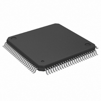
Manufacturer Part Number
MC68EC020AA25
Description
IC MPU 32BIT 25MHZ 100-QFP
Manufacturer
Freescale Semiconductor
Datasheet
1.MC68EC020AA16.pdf
(306 pages)
Specifications of MC68EC020AA25
Processor Type
M680x0 32-Bit
Speed
25MHz
Voltage
5V
Mounting Type
Surface Mount
Package / Case
100-QFP
Family Name
M68000
Device Core
ColdFire
Device Core Size
32b
Frequency (max)
25MHz
Instruction Set Architecture
RISC
Supply Voltage 1 (typ)
5V
Operating Supply Voltage (max)
5.25V
Operating Supply Voltage (min)
4.75V
Operating Temp Range
0C to 70C
Operating Temperature Classification
Commercial
Mounting
Surface Mount
Pin Count
100
Package Type
PQFP
Lead Free Status / RoHS Status
Lead free / RoHS Compliant
Features
-
Lead Free Status / Rohs Status
RoHS Compliant part
Electrostatic Device
Available stocks
Company
Part Number
Manufacturer
Quantity
Price
Company:

Part Number:
MC68EC020AA25
Manufacturer:
Freescale Semiconductor
Quantity:
10 000
Company:
Part Number:
MC68EC020AA25R
Manufacturer:
Freescale Semiconductor
Quantity:
10 000


3.6 ASYNCHRONOUS BUS CONTROL SIGNALS
The following signals control synchronous bus transfer operations for the
MC68020/EC020. Note that OCS, ECS, and DBEN are implemented in MC68020 and not
implemented in the MC68EC020.
Operand Cycle Start (OCS, MC68020 only)
External Cycle Start (ECS, MC68020 only)
Read/Write (R/ W)
Read-Modify-Write Cycle (RMC)
Address Strobe (AS)
Data Strobe (DS)
3- 4
This output signal indicates the beginning of the first external bus cycle for an instruction
prefetch or a data operand transfer. OCS is not asserted for subsequent cycles that are
performed due to dynamic bus sizing or operand misalignment. Refer to Section 5 Bus
Operation for information about the relationship of OCS to bus operation.
OCS is not implemented in the MC68EC020.
This output signal indicates the beginning of a bus cycle of any type. Refer to Section 5
Bus Operation for information about the relationship of ECS to bus operation.
ECS is not implemented in the MC68EC020.
This three-state output signal defines the type of bus cycle. A high level indicates a read
cycle; a low level indicates a write cycle. Refer to Section 5 Bus Operation for
information about the relationship of R/ W to bus operation.
This three-state output signal identifies the current bus cycle as part of an indivisible
read-modify-write operation; it remains asserted during all bus cycles of the read-
modify-write operation. Refer to Section 5 Bus Operation for information about the
relationship of RMC to bus operation.
This three-state output signal indicates that a valid address is on the address bus. The
FC2–FC0, SIZ1, SIZ0, and R /W signals are also valid when AS is asserted. Refer to
Section 5 Bus Operation for information about the relationship of AS to bus operation.
During a read cycle, this three-state output signal indicates that an external device
should place valid data on the data bus. During a write cycle, DS indicates that the
MC68020/EC020 has placed valid data on the bus. During two-clock synchronous write
cycles, the MC68020/EC020 does not assert DS . Refer to Section 5 Bus Operation for
more information about the relationship of DS to bus operation.
M68020 USER’S MANUAL
MOTOROLA
Related parts for MC68EC020AA25
Image
Part Number
Description
Manufacturer
Datasheet
Request
R

Part Number:
Description:
Manufacturer:
Freescale Semiconductor, Inc
Datasheet:
Part Number:
Description:
Manufacturer:
Freescale Semiconductor, Inc
Datasheet:
Part Number:
Description:
Manufacturer:
Freescale Semiconductor, Inc
Datasheet:
Part Number:
Description:
Manufacturer:
Freescale Semiconductor, Inc
Datasheet:
Part Number:
Description:
Manufacturer:
Freescale Semiconductor, Inc
Datasheet:
Part Number:
Description:
Manufacturer:
Freescale Semiconductor, Inc
Datasheet:
Part Number:
Description:
Manufacturer:
Freescale Semiconductor, Inc
Datasheet:
Part Number:
Description:
Manufacturer:
Freescale Semiconductor, Inc
Datasheet:
Part Number:
Description:
Manufacturer:
Freescale Semiconductor, Inc
Datasheet:
Part Number:
Description:
Manufacturer:
Freescale Semiconductor, Inc
Datasheet:
Part Number:
Description:
Manufacturer:
Freescale Semiconductor, Inc
Datasheet:
Part Number:
Description:
Manufacturer:
Freescale Semiconductor, Inc
Datasheet:
Part Number:
Description:
Manufacturer:
Freescale Semiconductor, Inc
Datasheet:
Part Number:
Description:
Manufacturer:
Freescale Semiconductor, Inc
Datasheet:
Part Number:
Description:
Manufacturer:
Freescale Semiconductor, Inc
Datasheet: